Display panel and display device
A display panel and display area technology, which is applied to semiconductor devices, electrical components, circuits, etc., can solve the problems such as the inability to further reduce the frame area of the display panel, the difficulty in realizing the full screen of the display panel display area, and the reduction of the display quality of the display panel, etc. Achieve the effect of improving display quality, eliminating edge aliasing, and reducing edge aliasing
- Summary
- Abstract
- Description
- Claims
- Application Information
AI Technical Summary
Problems solved by technology
Method used
Image
Examples
Embodiment 1
[0062] like Figure 6a1 , Figure 6a2 , Figure 6b1 , Figure 6b2 As shown, the extending direction of the first conductive traces 1110 in the direction perpendicular to the array substrate is the same, and since the pixel units located in the edge display area need to be connected with the pixel units of the same color located in the central display area, therefore, In the display panel provided by the embodiment of the present application, the arrangement order of the colors of the pixel units 03 located in the edge display area 022 is the pixel unit 03 located in the central display area 021 and connected to the pixel units 03 located in the edge display area 022 The colors are arranged in reverse order.
[0063] Specifically, such as Figure 6a1 , Figure 6a2 As shown, all the first conductive traces 1110 are arranged along the lateral extension direction in the direction perpendicular to the array substrate, and the arrangement order of the colors of the pixel units ...
Embodiment 2
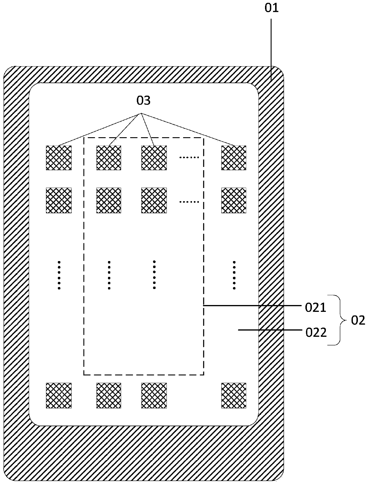
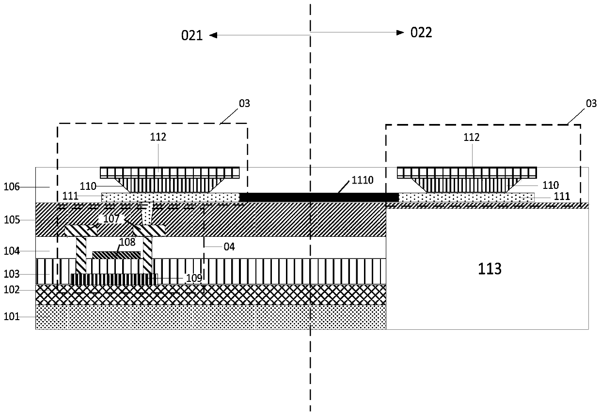
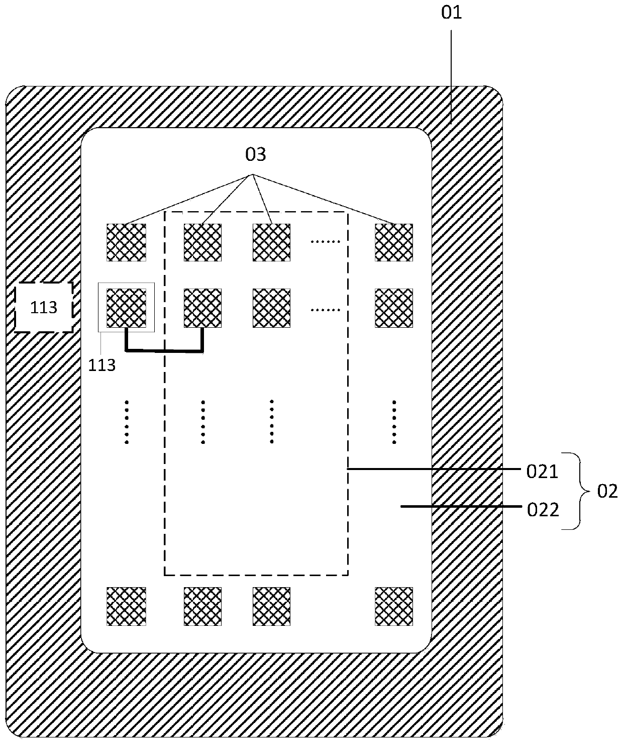
[0071] Such as Figure 7 As shown, the display panel provided by the embodiment of the present application includes a display area (such as figure 1 Shown display area 02) and non-display area (such as figure 1 shown in the non-display area 01), wherein the display area is divided into a central display area 021 and an edge display area 022, and a plurality of pixel units 03 are arranged in the display area, and the pixel units 03 include: a first electrode 111, and the The second electrode 112 opposite to the first electrode 111, and the light emitting layer 110 between the first electrode 111 and the second electrode 112; the display panel also includes: a base substrate 101 located on the base substrate 101 The buffer layer 102 on the side close to the pixel unit 03, the gate insulating layer 103 located on the side of the buffer layer 102 close to the pixel unit 03, the interlayer insulating layer 104 located on the side of the gate insulating layer 103 close to the pixel...
PUM
 Abstract
Description
Claims
Application Information
 - R&D Engineer
- R&D Manager
- IP Professional
- Industry Leading Data Capabilities
- Powerful AI technology
- Patent DNA Extraction
Browse by: Latest US Patents, China's latest patents, Technical Efficacy Thesaurus, Application Domain, Technology Topic, Popular Technical Reports.
© 2024 PatSnap. All rights reserved.Legal|Privacy policy|Modern Slavery Act Transparency Statement|Sitemap|About US| Contact US: help@patsnap.com


