
Data processing method among multiple FPGA chips and conversion device

A data processing and conversion device technology, applied in data exchange network, digital transmission system, error prevention, etc., can solve the problems of no multiple chip connections, complexity, large interface signal width, etc.

Active Publication Date: 2018-03-09
深圳市楠菲微电子有限公司
View PDF10 Cites 5 Cited by
  • Summary
  • Abstract
  • Description
  • Claims
  • Application Information

AI Technical Summary

Problems solved by technology

However, generally speaking, due to the complexity and diversity of ASIC chip functions, it is difficult to make a clear division when dividing a large-scale ASIC chip into subsystems, so that the interface signals between each subsystem can be kept simple.
Moreover, in many cases, the interface signal width between each subsystem is relatively large, and the FPGA chip does not have enough pins to realize the connection between multiple chips

Method used


Image

  • Data processing method among multiple FPGA chips and conversion device
  • Data processing method among multiple FPGA chips and conversion device
  • Data processing method among multiple FPGA chips and conversion device

Examples


Embodiment Construction

[0092] The specific implementation manners of the embodiments of the present invention will be described in detail below in conjunction with the accompanying drawings. It should be understood that the specific implementation manners described here are only used to illustrate and explain the embodiments of the present invention, and are not intended to limit the embodiments of the present invention.

[0093] When logically dividing a large ASIC chip, it is necessary to cut between main functional components according to the flow direction of data. In this way, the signal interface between the cut modules is relatively simple, and data transmission across FPGA chips is easy. In general, data interfaces are divided into the following types:

[0094] (1) Data interface with flow control

[0095] In ASIC chip design, if the data interface between two modules has a flow control function, it generally adopts a credit value-based flow control mechanism. Under this flow control mech...


PUM


Abstract

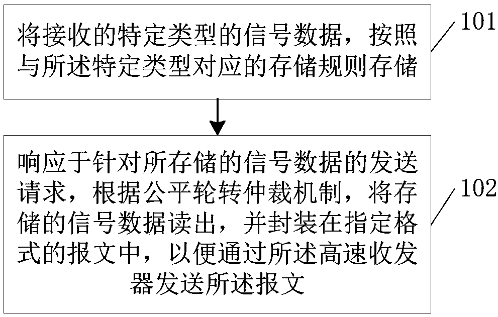
The embodiment of the invention provides a data processing method among multiple FPGA chips and a conversion device, and belongs to the technical field of FPGA chips. The data transmission problem inthe process of verifying an ASIC chip by multiple FPGA chips in the prior art is solved. The method is applied to the conversion device of one FPGA chip, and the conversion device is used for transmitting data between a data interface of the corresponding FPGA chip and a high-speed transceiver. The method includes the steps that a message to be sent is prepared, wherein received signal data of thespecific type is stored according to the storage rule corresponding to the specific type; responding to the sending request for the stored signal data, the stored signal data is read out according tothe fair round-robin arbitration mechanism and encapsulated in a message in a specified format, so that the message is sent by the high-speed transceiver conveniently. The embodiment of the inventionis applied to the data transmission process among the multiple FPGA chips.

Description

technical field [0001] The present invention relates to the technical field of FPGA (Field Programmable Gate Array, Field Programmable Gate Array) chips, in particular to a data processing method and device between multiple FPGA chips. Background technique [0002] In the design and verification process of large-scale ASIC (Application Specific Integrated Circuit, application-specific integrated circuit) chips, the use of software simulation methods for chip function verification is often limited due to slow verification speed and difficulty in expanding the scale. In order to test and evaluate the function and performance of the chip, it is often necessary to design a corresponding FPGA verification system, so as to speed up the verification progress, increase the verification scale and scenarios, discover deep-seated design problems as early as possible, and provide software and applications with available data in advance. development and testing platform. [0003] The cu...

Claims


Application Information

Patent Timeline
IPC IPC(8): H04L12/933H04L12/951H04L1/00H04L47/43
CPCH04L1/0061H04L49/109H04L49/9057
Inventor 王克非齐星云陈梨王志奇朱峰詹晋川
Owner 深圳市楠菲微电子有限公司
Learn More