A power module ceramic liner
A ceramic liner and power module technology, applied in the field of power module ceramic liner structure, can solve the problems of large inductance, complex liner interconnection, stray circuit interconnection structure, etc., to reduce stray inductance and high process efficiency , the effect of flexible wiring
- Summary
- Abstract
- Description
- Claims
- Application Information
AI Technical Summary
Problems solved by technology
Method used
Image
Examples
Embodiment 1
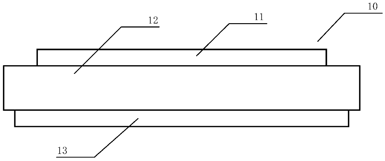
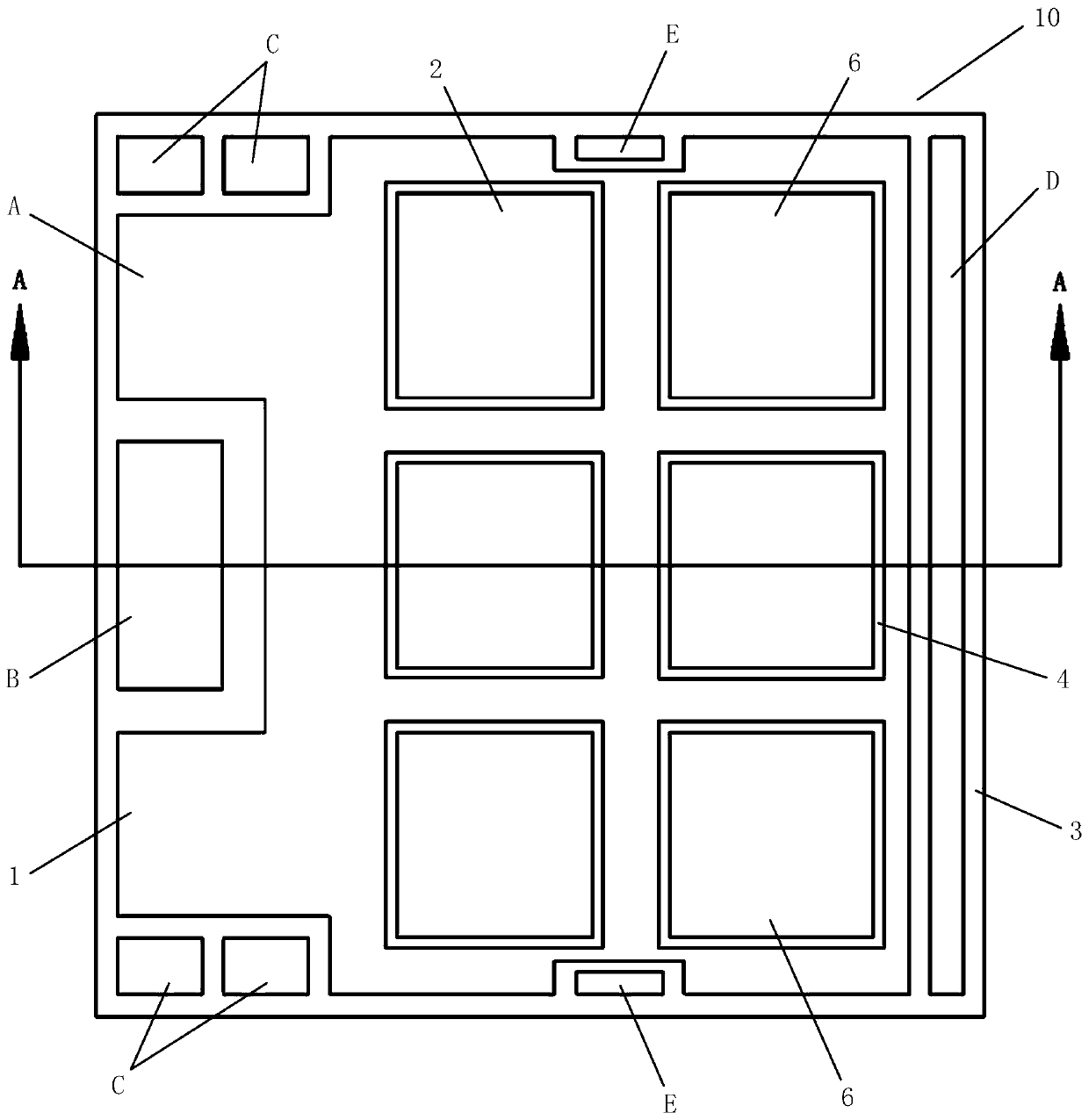
[0039] as attached image 3 As shown, a specific embodiment of a power module ceramic liner, the liner 10 adopts a multi-layer stacked structure with three layers of metal layers and two layers of ceramic layers arranged at intervals, and specifically includes: the first layer arranged in sequence from top to bottom Metal layer 1, second metal layer 2 and third metal layer 3. A first ceramic layer 4 is arranged between the first metal layer 1 and the second metal layer 2 , and a second ceramic layer 5 is arranged between the second metal layer 2 and the third metal layer 3 . Among them, the metal layer is made of copper, aluminum, gold, molybdenum and other materials, and the ceramic layer is made of AlN, Al 2 o 3 、Si 3 N 4 and other materials. as attached figure 2 As shown, the first metal layer 1 is arranged as an emitter region A (the emitter region A is also welded with emitter busbars) and a control signal terminal region C which are isolated from each other. The ...
Embodiment 2
[0046] as attached Figure 6 As shown, a specific embodiment of a power module ceramic liner, the liner 10 includes: a first metal layer 1 , a second metal layer 2 and a third metal layer 3 arranged in sequence from top to bottom. A first ceramic layer 4 is arranged between the first metal layer 1 and the second metal layer 2 , and a second ceramic layer 5 is arranged between the second metal layer 2 and the third metal layer 3 . The first metal layer 1 is set as the emitter area A and the control signal terminal area C which are isolated from each other, and the second metal layer 2 is set as the collector area B. Grooves 6 for mounting the first power chip 20 and the second power chip 30 are formed on the upper surface of the substrate 10 along the thickness direction, and the grooves 6 extend from the first metal layer 1 to the second metal layer 2 . The groove 6 can pass through the first ceramic layer 4 from the first metal layer 1, and extend to the upper surface of the...
PUM
| Property | Measurement | Unit |
|---|---|---|
| size | aaaaa | aaaaa |
Abstract
Description
Claims
Application Information
 - R&D
- Intellectual Property
- Life Sciences
- Materials
- Tech Scout
- Unparalleled Data Quality
- Higher Quality Content
- 60% Fewer Hallucinations
Browse by: Latest US Patents, China's latest patents, Technical Efficacy Thesaurus, Application Domain, Technology Topic, Popular Technical Reports.
© 2025 PatSnap. All rights reserved.Legal|Privacy policy|Modern Slavery Act Transparency Statement|Sitemap|About US| Contact US: help@patsnap.com


