Method for acquiring liquid crystal display panel defect location and liquid crystal display panel defect positioning device

A liquid crystal display panel and defect location technology, applied in the direction of instruments, nonlinear optics, optics, etc., can solve the problems of low operating efficiency and lack of pertinence of operators, and achieve the effects of improving operating efficiency, reducing losses, and avoiding missed inspections

Active Publication Date: 2019-07-02
SHENZHEN CHINA STAR OPTOELECTRONICS SEMICON DISPLAY TECH CO LTD
View PDF6 Cites 0 Cited by
  • Summary
  • Abstract
  • Description
  • Claims
  • Application Information

AI Technical Summary

Problems solved by technology

[0004] Since the imaging of the liquid crystal display panel must rely on polarized light, polarizers are attached to both sides of the array substrate and the color filter substrate. But in the prior art, after tearing off the polarizer, the operator just checks whether there is any foreign matter remaining on the surface of the entire liquid crystal display panel and wipes it, or directly wipes the entire surface of the liquid crystal display panel. Low, not targeted, if the residual foreign matter on the LCD panel is not wiped clean, it will be reworked again after reattaching the polarizer

Method used


Image

  • Method for acquiring liquid crystal display panel defect location and liquid crystal display panel defect positioning device
  • Method for acquiring liquid crystal display panel defect location and liquid crystal display panel defect positioning device
  • Method for acquiring liquid crystal display panel defect location and liquid crystal display panel defect positioning device

Examples


Embodiment Construction

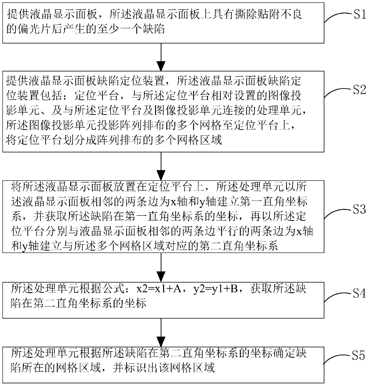
[0031] In order to further illustrate the technical means adopted by the present invention and its effects, the following describes in detail in conjunction with preferred embodiments of the present invention and accompanying drawings.

[0032] see figure 1 , the present invention provides a kind of method that obtains the defect position of liquid crystal display panel, comprises the following steps:

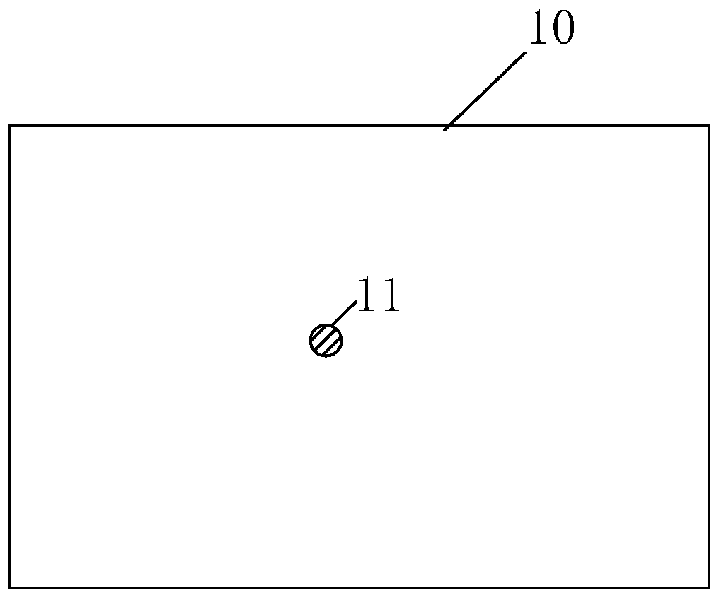
[0033] Step S1, please refer to figure 2 , providing a liquid crystal display panel 10, the liquid crystal display panel 10 has at least one defect 11 generated after the poorly attached polarizer is torn off;

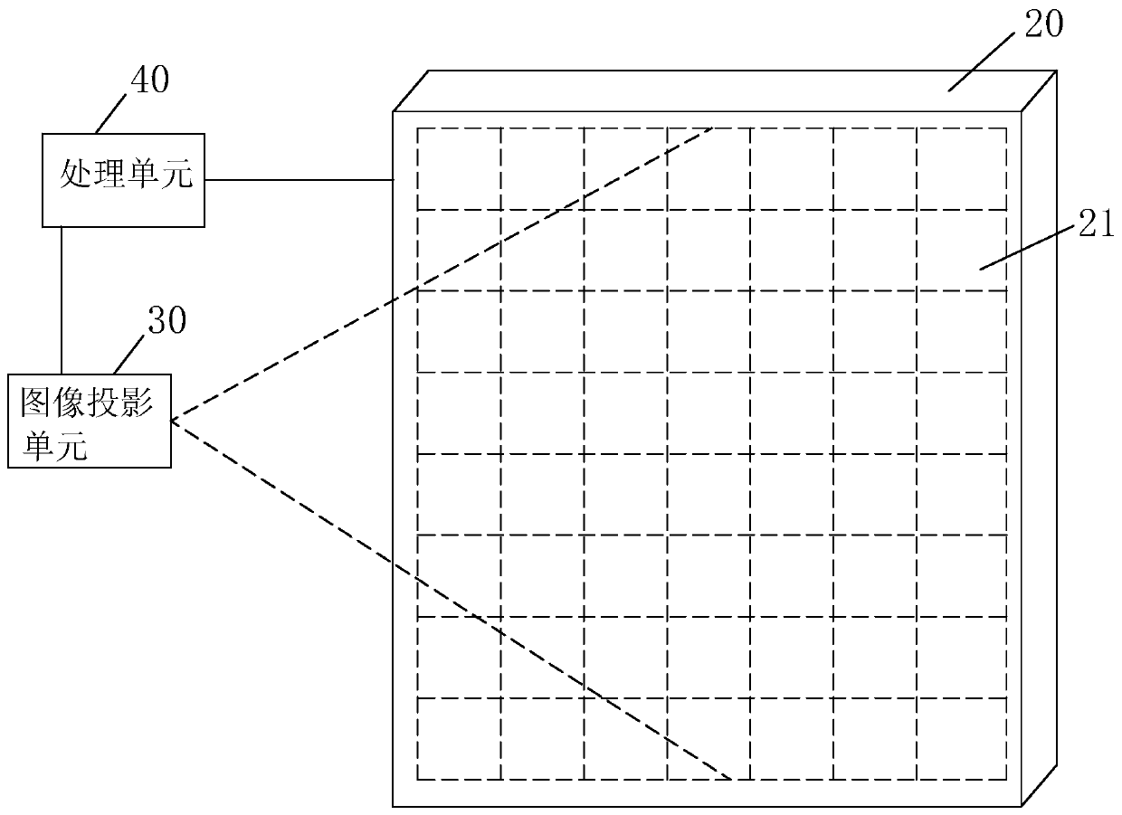
[0034] Step S2, please refer to image 3 , providing a liquid crystal display panel defect positioning device, said liquid crystal display panel defect positioning device comprising: a positioning platform 20, an image projection unit 30 arranged opposite to the positioning platform 20, and connected to the positioning platform 20 and the image projection unit 30 Th...


PUM


Abstract

A method for obtaining a defect position of a liquid crystal display panel (10) and a liquid crystal display panel (10) defect positioning device. The method comprises: a processing unit (40) establishes a first rectangular coordinate system with two adjacent sides of the liquid crystal display panel (10) as an x axis and a y axis, obtains coordinates (x1, y1) of a defect (11) of the liquid crystal display panel (10) in the first rectangular coordinate system, then establishes a second rectangular coordinate system with two sides of a positioning platform (20) respectively parallel to two adjacent sides of the liquid crystal display panel (10) as an x axis and a y axis, and calculates coordinates (x2, y2) of the defect (11) in the second rectangular coordinate system according to a linear distance between the second rectangular coordinate system and the first rectangular coordinate system; an image projection unit (30) then divides the positioning platform (20) into multiple grid regions (21) corresponding to the second rectangular coordinate system and arranged in an array; the processing unit (40) determines and identifies a grid region (21) where the defect (11) is located. An operator can conveniently and accurately check the defect (11) on the liquid crystal display panel (10), the operating efficiency is improved, multiple times of processing conducted on the liquid crystal display panel (10) are prevented, and accordingly the loss of polarizers is reduced.

Description

technical field [0001] The invention relates to the field of display technology, in particular to a method for obtaining defect positions of a liquid crystal display panel and a defect positioning device for a liquid crystal display panel. Background technique [0002] With the development of display technology, liquid crystal displays (Liquid Crystal Display, LCD) and other flat display devices are widely used in mobile phones, televisions, personal Various consumer electronic products such as digital assistants, digital cameras, notebook computers, and desktop computers have become the mainstream of display devices. [0003] Generally, a liquid crystal display device includes a housing, a liquid crystal display panel disposed in the housing, and a backlight module disposed in the housing. Among them, the structure of the liquid crystal display panel is mainly composed of an array substrate (Thin FilmTransistor Array Substrate, TFT Array Substrate), a color filter substrat...

Claims


Application Information

Patent Timeline
Patent Type & Authority Patents(China)
IPC IPC(8): G02F1/13
CPCG02F1/13
Inventor 谢军
Owner SHENZHEN CHINA STAR OPTOELECTRONICS SEMICON DISPLAY TECH CO LTD
Why Eureka
Try Eureka