Ultra-small-size glue-filling surface-mount LED packaging unit

A technology of LED packaging and adhesive patch, applied in electrical components, electric solid devices, circuits, etc., can solve the problem that the LED display cannot be viewed at close range, the light output of high-density LED display is scattered, and the LED display cannot be applied, etc. problem, to achieve the effect of small dot pitch, light concentration, and reduced package size

Inactive Publication Date: 2018-01-09
MIANYANG XINYANG INTPROP CO LTD
View PDF2 Cites 0 Cited by
  • Summary
  • Abstract
  • Description
  • Claims
  • Application Information

AI Technical Summary

Problems solved by technology

However, due to the size of the traditional SMD LED package size and heat dissipation problems, the LED display cannot be as convenient and close-up as other display media, making the LED display unable to obtain a good application in the field of indoor high-definition display.
[0003] In order to reduce the packaging size of LED lamp beads and realize the requirements of small dot pitch and high definition of LED display, the LED lamp beads used in the existing LED ultra-high-definition indoor display screens are all PCB structures, and the lamp beads are integrally formed, unified Cutting, although this packaging method solves the problem of large package size of traditional SMD LEDs, but due to the poor light-gathering effect of the packaging structure itself, the resulting high-density LED display has problems such as light dispersion, high energy consumption, and light pollution.

Method used


Image

  • Ultra-small-size glue-filling surface-mount LED packaging unit
  • Ultra-small-size glue-filling surface-mount LED packaging unit
  • Ultra-small-size glue-filling surface-mount LED packaging unit

Examples


Embodiment 1

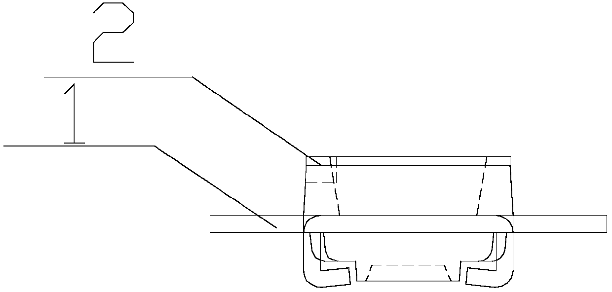
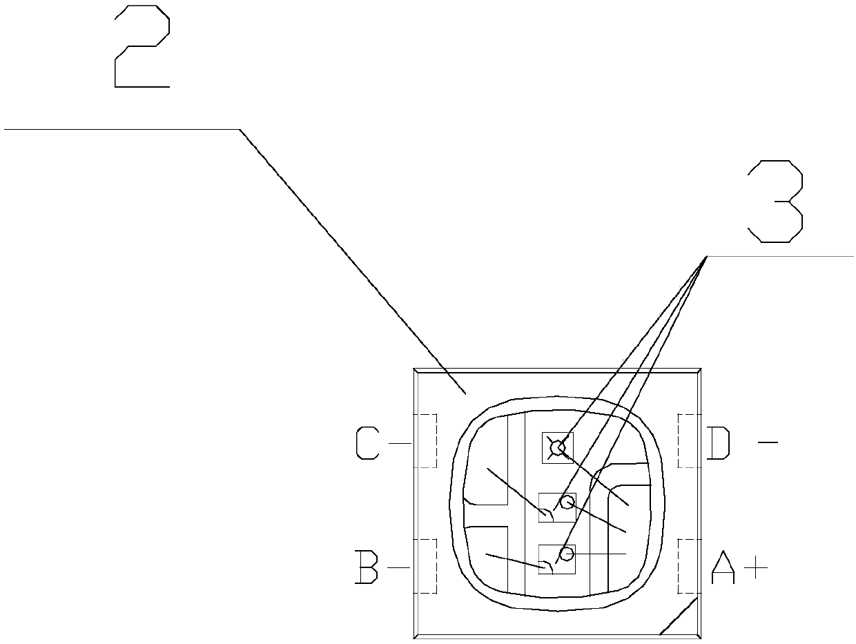
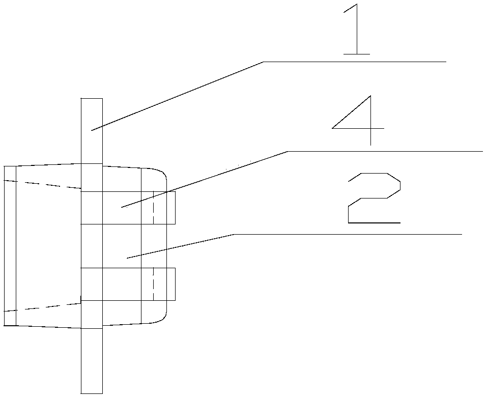
[0020] Such as Figure 1-2 As shown, the present invention includes a packaging support 1, a packaging bowl 2 installed in the middle of the packaging support 1, a wire bonding area 4 and a chip 3 packaged in the packaging bowl 2. There are many chips 3, all located in the same On a plane and arranged on the same straight line; the packaged cup 2 is filled with glue, and a plurality of welding wire areas 4 are arranged at the bottom of the packaged cup 2 . The chip of this embodiment has three chips of red, green and blue, which are arranged in a line from top to bottom. , which avoids the drawbacks of the existing character-shaped chip arrangement, where the three chips block light from each other at different angles in the horizontal direction, and provides better display consistency for the display screen.

Embodiment 2

[0022] Such as Figure 2-3 As shown, this embodiment is based on the embodiment 1, and the preferred specific structure is as follows: the wire bonding area 4 on the packaging cup 2 is distributed symmetrically, and the bottom of the wire bonding area 4 is connected to the packaging bracket 1 . The bracket used is an all-black bracket, and the welding line area can be retracted to effectively avoid solder reflection in the welding line area. Compared with full-color Chip LEDs, it has high contrast, bright colors, better light-gathering effect, and softer light. The display effect is delicate and the color reproduction is high, fully meeting the quality requirements of high-end LED displays.

Embodiment 3

[0024] Such as figure 1 As shown, this embodiment adds the following technical features on the basis of any one of the above embodiments: the bonding wire area 4 includes a positive electrode bonding wire area and three negative electrode bonding wire areas, and the positive electrode bonding wire area A+ is located on the right side of the packaging bowl cup 2 Below, there are two negative electrode bonding areas B- and C- on the left side of the packaged cup 2 and a negative electrode bonding area D- on the upper right side of the packaged cup 2 . The positive electrodes of the pins on each chip 3 are welded in the same positive electrode bonding area, and the negative electrodes of the pins are welded in different negative electrode bonding areas. The negative poles of the pins of all chips 3 arranged on the same straight line are welded clockwise in the negative electrode welding line area. The packaging support 1 is rectangular and crosses the middle of the packaging cup...


PUM


Abstract

The invention discloses an ultra-small-size glue-filling surface-mount LED packaging unit. The packaging unit comprises a packaging bracket, a packaging bowl cup installed in the middle of the packaging bracket, bonding wire zones, and wafers packaged in the packaging bowl cup packaged in the packaging bowl cup. Multiple wafers are arranged on the same plane and are distributed on the same straight line. The packaging bowl cup is poured and filled with glue; and a plurality of bonding wire zones are arranged at the bottom of the packaging bowl cup. According to the invention, on the basis of the top light-emitting structure, the appearance dimension is reduced on the premise that the light emitting angle of the product is not changed and the product brightness is not reduced.

Description

technical field [0001] The invention relates to the field of packaging of LED light-emitting diodes, in particular to an ultra-small-sized glue-filled patch LED package. Background technique [0002] Nowadays, LED electronic display has become a leader in many display media due to its bright colors, wide dynamic range, high brightness, long life, stable and reliable operation, etc. It is widely used in sports venues, cities and public squares, transportation, corporate image promotion, commercial advertisements, etc. Sports venues have a long viewing distance and high requirements for ambient brightness. LED display screens can well meet this special requirement, ensuring that the audience can obtain clear and vivid color images, and bringing unlimited visual enjoyment to the audience. However, due to the size and heat dissipation of traditional SMD LED packages, LED displays cannot be viewed at close range as conveniently as other display media, making LED displays unable ...

Claims


Application Information

Patent Timeline
Patent Type & Authority Applications(China)
IPC IPC(8): H01L25/075H01L33/48H01L33/52H01L33/62
CPCH01L2224/48247H01L2224/49113
Inventor 龚平
Owner MIANYANG XINYANG INTPROP CO LTD
Why Eureka
Try Eureka