Imaging element, multilayer imaging element and imaging device
An image sensor and carrier blocking layer technology, which is applied in radiation control devices, electric solid state devices, semiconductor devices, etc., can solve the problems of reduced photoelectric conversion efficiency, no mention of image sensors, and no spectral characteristics involved. Dark current, good external quantum efficiency and spectroscopic characteristics, effect of improving dark current-voltage characteristics
- Summary
- Abstract
- Description
- Claims
- Application Information
AI Technical Summary
Problems solved by technology
Method used
Image
Examples
Embodiment 2
[0048] 3. Embodiment 2 (variation of Embodiment 1)
[0049] 4. Embodiment 3 (variations of Embodiment 1 and Embodiment 2, the stacked image sensor of the present invention, and the camera module according to the second aspect of the present invention)
[0050] 5. Other
[0051] Outline of the image sensor according to the first aspect to the third aspect of the present invention, the stacked imaging device according to the present invention, and the imaging module according to the first aspect to the second aspect of the present invention
[0052] A configuration in which three types of image sensors are stacked in the vertical direction can be mentioned. Specifically, the three image sensors include an image sensor according to one of the first to third aspects of the present invention (for convenience, it will be referred to as a "blue image sensor"), and an image sensor according to the first aspect of the present invention. ~ Another image sensor of one of the third aspe...
Embodiment 1
[0076] Embodiment 1 relates to the image sensor according to the first aspect to the third aspect of the present invention, and also relates to the camera module according to the first aspect of the present invention.
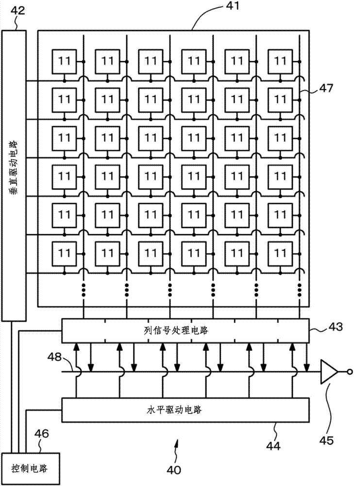
[0077] Such as figure 1 A and figure 1 As shown in the conceptual diagram of B, each image sensor 11 of Embodiment 1 includes at least a first electrode 21 , a second electrode 25 , an organic photoelectric conversion layer 23 and a carrier blocking layer 22 . Specifically, the first electrode 21 serves as an anode, the second electrode 25 serves as a cathode, and the carrier blocking layer 22 is disposed between the first electrode 21 and the organic photoelectric conversion layer 23 . More specifically, each image sensor 11 of Embodiment 1 consists of at least a first electrode (anode) 21, a carrier blocking layer (first carrier blocking layer) 22, an organic photoelectric conversion layer 23, and a second Two electrodes (cathode) 25 are formed. In additio...
Embodiment 3
[0159] Embodiment 3 is a modified example of the image sensor of Embodiments 1 and 2, and relates to the stack-type imaging device of the present invention and the imaging module according to the second aspect of the present invention. Specifically, the stacked image pickup device (longitudinal spectroscopic image pickup device) of Embodiment 3 is formed of at least two image sensors identical to one of those described in Embodiments 1 and 2, and the at least two Image sensors are stacked on top of each other. On the other hand, the camera module of Example 3 includes a plurality of such laminated camera devices. Specifically, such as Figure 7 As shown in the conceptual diagram of A, the laminated imaging device of Embodiment 3 has the following configuration: three image sensors (three sub-image sensors) composed of the blue image sensor, green image sensor, and red image sensor described in Embodiments 1 and pixels) are stacked vertically. Therefore, it is possible to ob...
PUM
| Property | Measurement | Unit |
|---|---|---|
| size | aaaaa | aaaaa |
| carrier mobility | aaaaa | aaaaa |
Abstract
Description
Claims
Application Information
 - R&D Engineer
- R&D Manager
- IP Professional
- Industry Leading Data Capabilities
- Powerful AI technology
- Patent DNA Extraction
Browse by: Latest US Patents, China's latest patents, Technical Efficacy Thesaurus, Application Domain, Technology Topic, Popular Technical Reports.
© 2024 PatSnap. All rights reserved.Legal|Privacy policy|Modern Slavery Act Transparency Statement|Sitemap|About US| Contact US: help@patsnap.com


