


Quick Research
Generate reliable direction feasibility study reports for your R&D in just a few steps.

Technical Q&A
Discover and master advanced knowledge NOW. Basics, ideas, possibilities, all at once.

Find Solutions
As an expert in R&D theories, this can generate solutions to your technical problems instantly.

Evaluate Feasibility
Analyze your overall solution with one click, know your potential R&D risks in advance.

Monitor Landscape
Get weekly tech updates, stay abreast of the latest tech innovations and key insights.
Processing system and method for shielding film
A processing system and processing method technology, applied in the fields of magnetic field/electric field shielding, devices for coating liquid on the surface, electrical components, etc., can solve problems affecting product performance, reduction of coating continuity, uneven coating, etc.
- Summary
- Abstract
- Description
- Claims
- Application Information
AI Technical Summary
Problems solved by technology
Method used
Image

Examples
Embodiment 1
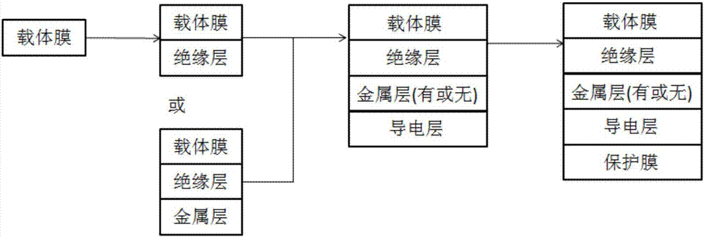
[0054] Please also refer to Figure 1-4 , figure 1 It is the processing flow chart of the shielding film in the prior art. In the prior art, the coating production of the shielding film is mainly to coat the insulating layer on the carrier film to obtain a semi-finished product, and coat the conductive layer glue on the outside of the semi-finished product, and finally in the The outer side of the conductive layer is pasted with a protective film to form a shielding film. In actual production, a metal layer can be selected to be processed on one side of the insulating layer according to needs.
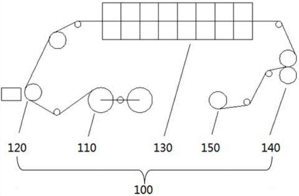
[0055] Such as figure 2 As shown, this embodiment provides a shielding film processing system, including a semi-finished product processing system 100 and a finished product processing system 200, specifically:
[0056] The semi-finished product processing system 100 is used for coating an insulating layer on the carrier film to make a semi-finished product of the shielding film;
...
Embodiment 2
[0068] This embodiment provides a method for processing a shielding film using the shielding film processing system in Embodiment 1, including:
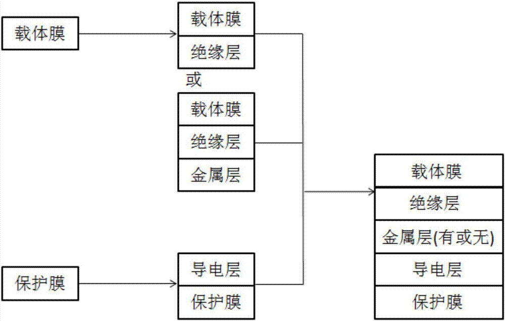
[0069] Coating an insulating layer on the carrier film to produce a semi-finished product, which can be completed by the semi-finished product processing system 100;
[0070] A conductive layer is coated on the protective film, and the side of the conductive layer facing away from the protective film is combined with the side of the insulating layer facing away from the carrier film to make a finished product. The finished product can be finished by the finished product processing system 200 .
[0071] Coating an insulating layer on a carrier film to make a semi-finished product is:
[0072] Coating an insulating layer on one side of the carrier film, the carrier film can be sent to the first coating device 120 through the first sending device 110, and then utilize the coating head of the first coating device 120 to coat the insulati...
PUM
 Abstract
Description
Claims
Application Information
 - R&D Engineer
- R&D Manager
- IP Professional
- Industry Leading Data Capabilities
- Powerful AI technology
- Patent DNA Extraction
Browse by: Latest US Patents, China's latest patents, Technical Efficacy Thesaurus, Application Domain, Technology Topic, Popular Technical Reports.
© 2024 PatSnap. All rights reserved.Legal|Privacy policy|Modern Slavery Act Transparency Statement|Sitemap|About US| Contact US: help@patsnap.com