Flash memory device capable of avoiding data wiping error

A technology of data erasing and flash memory, which is applied in the direction of information storage, static memory, read-only memory, etc., can solve the problems of reducing erasing efficiency, accelerating the loss of NAND flash memory devices, reducing the durability of storage units, and achieving the goal of overcoming the aggravated loss Effect

Inactive Publication Date: 2017-12-22
DOSILICON CO LTD
View PDF4 Cites 0 Cited by
  • Summary
  • Abstract
  • Description
  • Claims
  • Application Information

AI Technical Summary

Problems solved by technology

[0002] Memory (Memory) is a memory device used to store information in modern information technology. It is widely used in notebooks, smart phones and various terminal devices. Memory is divided into NAND flash memory devices and NOR flash memory devices on the circuit. When erasing it in a NAND flash memory device, the existing method is to use one erase operation to erase the NAND flash memory device. The disadvantage it brings is that the storage cells in the NAND flash memory device will be excessively erased. Therefore, when performing the next erasing operation, the number of erasing cycles needs to be increased, while reducing the erasing efficiency, the durability of the storage unit is also reduced, and the wear and tear of the NAND flash memory device is accelerated.

Method used


Image

  • Flash memory device capable of avoiding data wiping error
  • Flash memory device capable of avoiding data wiping error
  • Flash memory device capable of avoiding data wiping error

Examples


Embodiment Construction

[0036] The following will clearly and completely describe the technical solutions in the embodiments of the present invention with reference to the accompanying drawings in the embodiments of the present invention. Obviously, the described embodiments are only some, not all, embodiments of the present invention. Based on the embodiments of the present invention, all other embodiments obtained by persons of ordinary skill in the art without creative efforts fall within the protection scope of the present invention.

[0037] It should be noted that, in the case of no conflict, the embodiments of the present invention and the features in the embodiments can be combined with each other.

[0038] The present invention will be further described below in conjunction with the accompanying drawings and specific embodiments, but not as a limitation of the present invention.

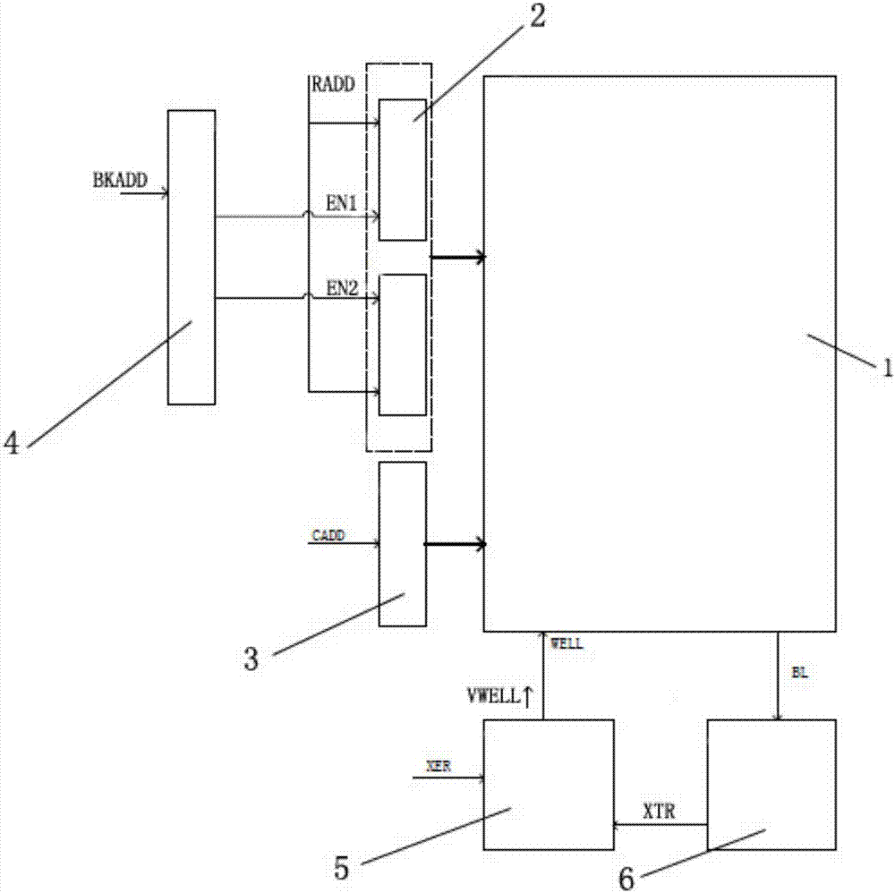
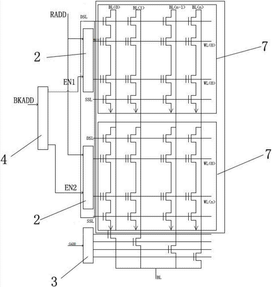
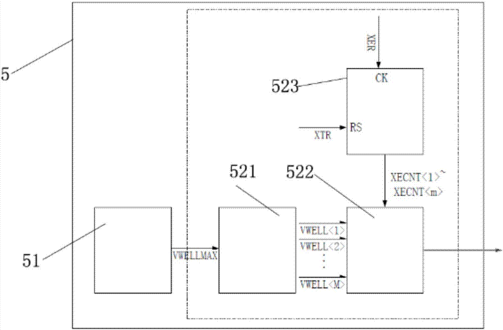
[0039] The technical solution of the present invention includes a flash memory device that avoids excessive eras...


PUM


Abstract

The invention provides a flash memory device capable of avoiding data wiping error, which is applied for flash memory wiping. A memory array includes a plurality of memory units. The flash memory device includes: a data wiping unit, in which wiping voltages in several stages from high to low are pre-formed, and then according to a wiping signal inputted from exterior, a stage of wiping voltage is outputted so as to perform data wiping to an activated memory unit; and a data detection unit, which detects the memory unit to determine whether data wiping is successfully performed or not when the memory unit is wiped, and if data wiping is in failure, the data detection unit sends a second detection signal to the data wiping unit; the data wiping unit, when receiving the second detection signal, increases the wiping voltage by one stage than before, and then performs the data wiping to the activated memory unit again until the memory unit is wiped successfully. The flash memory device overcomes the defect of aggravated consumption due to excessive wiping of the memory units in the prior art.

Description

technical field [0001] The invention relates to the field of storage devices, in particular to a flash memory device for avoiding data erasing errors. Background technique [0002] Memory (Memory) is a memory device used to store information in modern information technology. It is widely used in notebooks, smart phones and various terminal devices. Memory is divided into NAND flash memory devices and NOR flash memory devices on the circuit. When erasing it in a NAND flash memory device, the existing method is to use one erase operation to erase the NAND flash memory device. The disadvantage it brings is that the storage cells in the NAND flash memory device will be excessively erased. Therefore, the number of erasing cycles needs to be increased when performing an erasing operation next time, and while erasing efficiency is reduced, the durability of the storage unit is also reduced, and wear and tear of the NAND flash memory device is accelerated. Contents of the inventio...

Claims


Application Information

Patent Timeline
Patent Type & Authority Applications(China)
IPC IPC(8): G11C16/14G11C16/34
CPCG11C16/14G11C16/3409G11C16/3495
Inventor 王文静康太京李炯尚朱家骅谢莺霞张纲何峻
Owner DOSILICON CO LTD
Why Eureka
Try Eureka