


Quick Research
Generate reliable direction feasibility study reports for your R&D in just a few steps.

Technical Q&A
Discover and master advanced knowledge NOW. Basics, ideas, possibilities, all at once.

Find Solutions
As an expert in R&D theories, this can generate solutions to your technical problems instantly.

Evaluate Feasibility
Analyze your overall solution with one click, know your potential R&D risks in advance.

Monitor Landscape
Get weekly tech updates, stay abreast of the latest tech innovations and key insights.
SMD surface mount support
A SMD, LED chip technology, applied in electrical components, circuits, semiconductor devices, etc., can solve the problems of poor structural stability, easily affected conductive areas, etc., to achieve the effect of simple and practical structure and changing current
- Summary
- Abstract
- Description
- Claims
- Application Information
AI Technical Summary
Problems solved by technology
Method used
Image

Examples
Embodiment 1
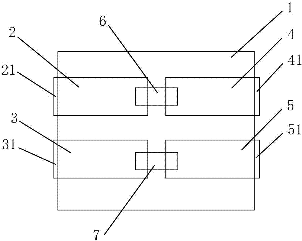
[0014] Such as figure 1 As shown, the present embodiment provides a kind of SMD patch support, including plastic base 1, and described plastic base 1 is provided with encapsulation platform and is arranged on the conductive sheet that is used for connecting LED chip on the encapsulation platform, and described encapsulation There are four conductive sheets on the table, and each conductive sheet extends from the inside to the outside along the packaging table to form conductive pins on both sides of the packaging table, and the packaging table is provided with positioning grooves matching the conductive sheets. The conductive sheet is embedded in the positioning groove and is flat with the end surface of the packaging table, and the plastic base 1 is a polymer non-conductive material.
[0015] The conductive sheet that this embodiment adopts is rectangular, with figure 1 As an example, the conductive sheet is divided into the first conductive sheet 2, the second conductive sh...
Embodiment 2
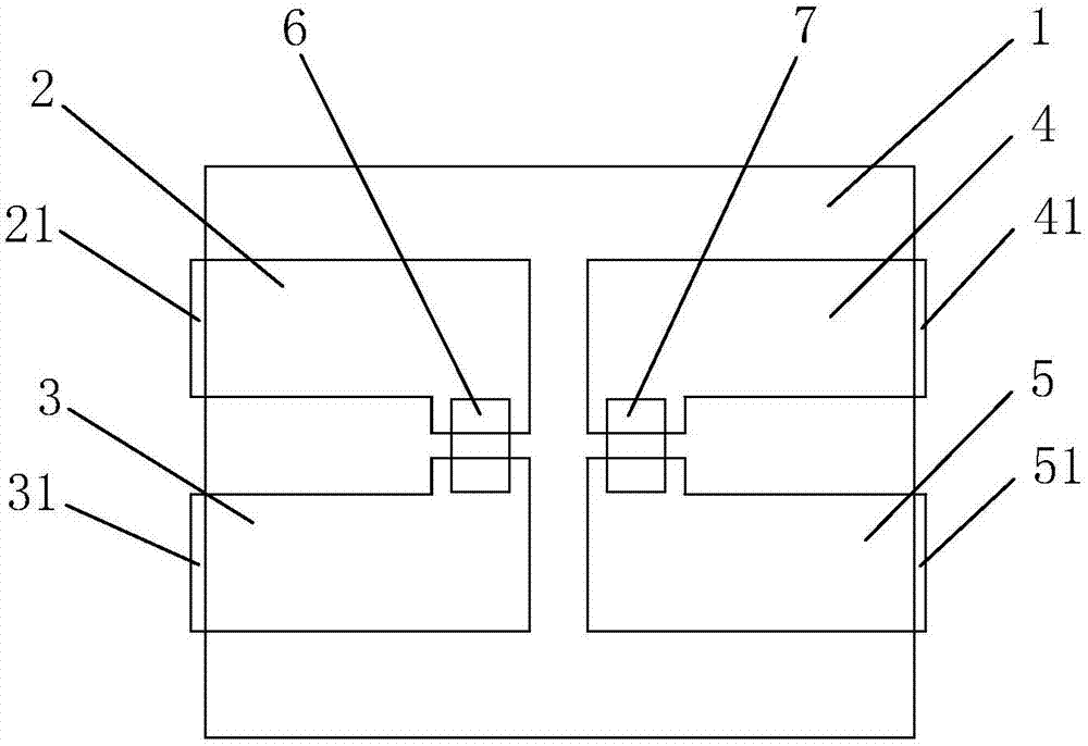
[0018] Such as figure 2 As shown, the difference between this embodiment and Embodiment 1 is that the conductive sheet adopts an L-shaped structure, wherein the L-shaped bottom ends of the first conductive sheet 2 and the second conductive sheet 3 are opposite and divided into one group, and the third conductive sheet 4 Opposite to the L-shaped bottom end of the fourth conductive sheet 5 and divided into another group, the first LED chip 6 is connected to the bottom position between the first conductive sheet 2 and the second conductive sheet 3, and the second LED chip 7 is connected to The bottom position between the second conductive sheet 3 and the fourth conductive sheet 5 . The series-parallel connection mode is the same as the first embodiment.
PUM
 Abstract
Description
Claims
Application Information
 - R&D Engineer
- R&D Manager
- IP Professional
- Industry Leading Data Capabilities
- Powerful AI technology
- Patent DNA Extraction
Browse by: Latest US Patents, China's latest patents, Technical Efficacy Thesaurus, Application Domain, Technology Topic, Popular Technical Reports.
© 2024 PatSnap. All rights reserved.Legal|Privacy policy|Modern Slavery Act Transparency Statement|Sitemap|About US| Contact US: help@patsnap.com