Circuit for improving parallel connection current distribution of power semiconductor device

A power semiconductor and device technology, applied in the field of power semiconductor parallel connection, can solve problems such as high cost and price, current level limitation, power semiconductor device damage, etc., to improve parallel current distribution, avoid direct damage, and reduce transient current distribution. The effect of balance

Inactive Publication Date: 2017-12-08
NORTH CHINA ELECTRIC POWER UNIV (BAODING)
View PDF2 Cites 5 Cited by
  • Summary
  • Abstract
  • Description
  • Claims
  • Application Information

AI Technical Summary

Problems solved by technology

First, the current level is limited. The current level of power semiconductor devices (including metal-oxide semiconductor field effect transistors (hereinafter referred to as MOSFETs), IGBTs, etc.) cannot meet the needs of system developers. In the special period that has not been launched, parallel connection is the main way to solve this demand
Second, due to economic cost constraints, even if devices with higher currents begin to enter the market, their cost and price are often relatively high, so it is more economical to use devices with small and medium power levels in parallel
[0003] At present, due to the immature manufacturing process of power semiconductor device materials, it is difficult to solve the problem of power semiconductor device parameter dispersion in a short period of time, and the parameter differences of power semiconductor devices cannot be completely consistent, resulting in power semiconductor device In the parallel connection mode, there may be problems of asynchronous switching and unbalanced current distribution between parallel power semiconductor devices. In severe cases, it will directly cause direct damage to power semiconductor devices due to large currents.

Method used


Image

  • Circuit for improving parallel connection current distribution of power semiconductor device
  • Circuit for improving parallel connection current distribution of power semiconductor device

Examples


Embodiment Construction

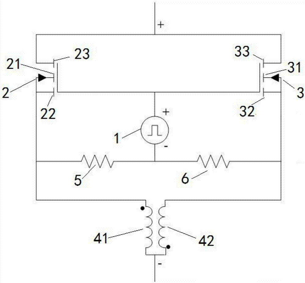
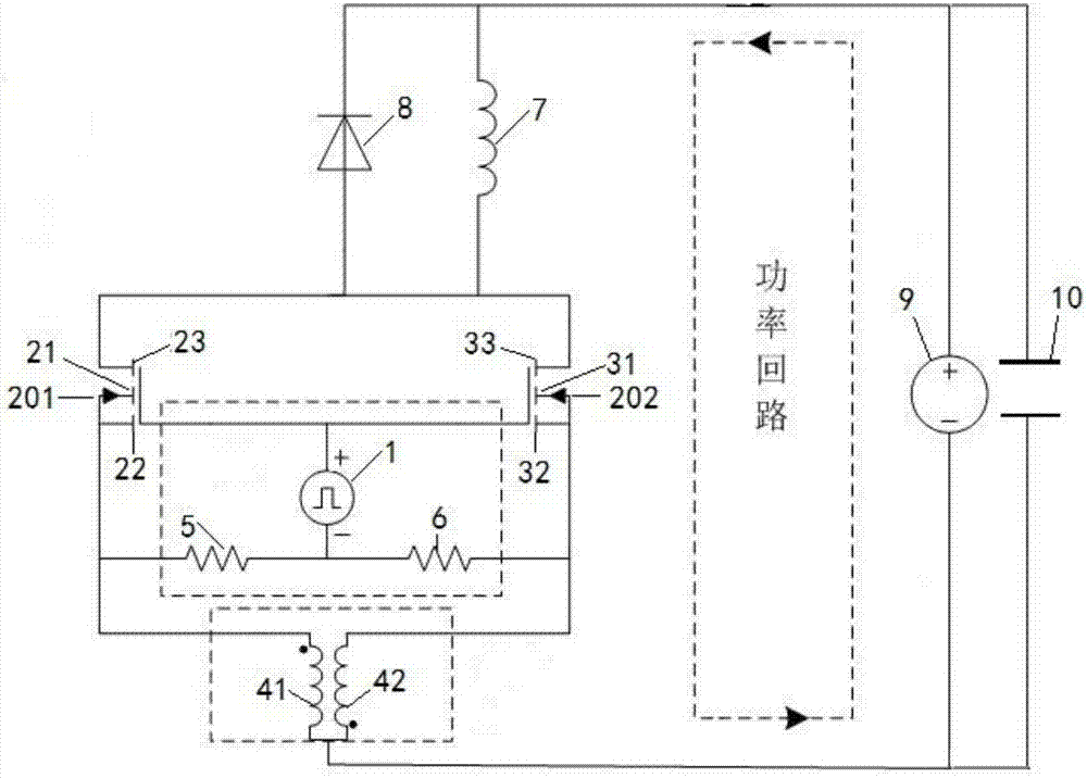
[0022] The following will clearly and completely describe the technical solutions in the embodiments of the present invention with reference to the accompanying drawings in the embodiments of the present invention. Obviously, the described embodiments are only some, not all, embodiments of the present invention. Based on the embodiments of the present invention, all other embodiments obtained by persons of ordinary skill in the art without making creative efforts belong to the protection scope of the present invention.

[0023] Compared with the prior art, at present, the transient current balance between parallel power semiconductor devices is mainly realized through an active delay compensation method. Active delay compensation method, directly obtains the current difference through PCB type Rogowski coils, current transformers and other measurement methods or indirectly extracts the current imbalance information through the voltage drop of stray inductance, and feeds back to...


PUM


Abstract

The circuit for improving parallel connection current distribution of a power semiconductor device. The circuit of the invention is improved on the basis of a traditional power semiconductor device parallel connection circuit and is particularly realized by adding inductors which are coupled in negative direction and have same inductance values on a source electrode side of each power semiconductor device. When the parallel connection power semiconductor devices are turned on, the two inductors which are coupled in negative directions can sense voltage drops which are different in direction and same in amplitude and can feed the voltage drops back to a driving unit. The power semiconductor device having a higher switching speed is reduced and the power semiconductor device having a lower switching speed is increased. Besides, resistors having same resistance values are inserted between source electrodes of the power semiconductor devices and a negative electrode of a driving unit, which can prevent the voltage drop from generating ultrahigh transient compensation current on a source electrode lead. As a result, the circuit for improving serial connection current distribution of the power semiconductor device can reduce transient current distribution maldistribution between power semiconductor devices which are connected in parallel and can prevents the power semiconductor device from direct damage due to big current.

Description

technical field [0001] The invention relates to the field of power semiconductor parallel connection, in particular to a circuit for improving the parallel current distribution of power semiconductor devices. Background technique [0002] In high-power power electronics applications, there are three main reasons for paralleling power requirements. First, the current level is limited. The current level of power semiconductor devices (including metal-oxide semiconductor field effect transistors (hereinafter referred to as MOSFETs), IGBTs, etc.) cannot meet the needs of system developers. In the special period that has not been launched, the parallel connection method is the main way to solve this demand. Second, economic cost constraints. Even if devices with higher currents start to enter the market, their cost and price are often relatively high. Therefore, it is more economical to use devices with low and medium power levels in parallel. Third, reliability requirements. L...

Claims


Application Information

Patent Timeline
Patent Type & Authority Applications(China)
IPC IPC(8): H03K17/082H03K17/567H03K17/687
CPCH03K17/0822H03K17/0828H03K17/567H03K17/687
Inventor 柯俊吉孙鹏黄华震邹琦赵志斌崔翔
Owner NORTH CHINA ELECTRIC POWER UNIV (BAODING)
Why Eureka
Try Eureka