Image collection system
An image acquisition system and image acquisition technology, applied in image acquisition, image communication, image data processing, etc., can solve problems such as poor imaging quality, high cost, and sensitivity to the external environment, and achieve the effect of improving efficiency and low power consumption
- Summary
- Abstract
- Description
- Claims
- Application Information
AI Technical Summary
Problems solved by technology
Method used
Image
Examples
Embodiment 1
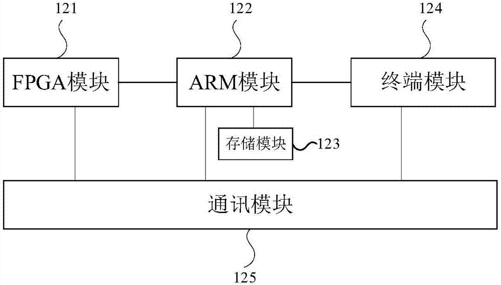
[0043] See figure 1 , figure 1 A structural block diagram of an image acquisition system provided by an embodiment of the present invention; the system includes:
[0044] Image source 11, used to generate source images;
[0045] The acquisition card 12 is electrically connected to the image source 11, and is used for encoding and analyzing the source image;
[0046] The system software 13 is used to control the image source 11 and the acquisition card 12 for image acquisition and transmission.
[0047] Specifically, the system software 13 may include acquisition card embedded software and host computer software; wherein, the acquisition card embedded software is installed on the acquisition card 12 for controlling the image source 11 and the acquisition card 12 for image acquisition and transmission; the upper computer The software is installed on the host computer electrically connected with the acquisition card 12, and is used for remote control of the image source 11 and...
Embodiment 2
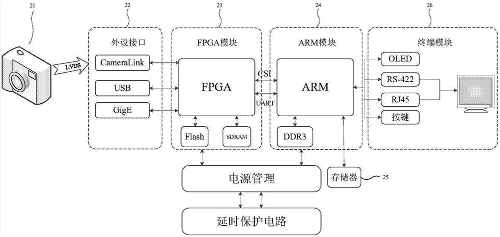
[0058] Further, on the basis of the above embodiments, for a clearer understanding, the principle of the image acquisition system will be described in detail below.
[0059] Specifically, see image 3 , image 3 A functional block diagram of an image acquisition system provided by another embodiment of the present invention; including: an image source 21 , a peripheral interface 22 , an FPGA module 23 , an ARM module 24 , a memory 25 and a terminal module 26 .
[0060] Preferably, the peripheral interface 22 is a CameraLink interface, a USB interface and a GigE interface.
[0061] Preferably, the memory 25 is an SSD memory with mSATA interface.
[0062] Preferably, see Figure 4 , Figure 4 A kind of FPGA module functional block diagram that another embodiment of the present invention provides; FPGA module 23 comprises the first conversion chip, the second conversion chip, FPGA chip and the first memory; Wherein, the first conversion chip and the first conversion chip are ...
Embodiment 3
[0074] Further, on the basis of the above embodiments, the following describes the image acquisition system in detail according to the design of the PCB board.
[0075] When designing printed circuit boards (PCB boards), first classify the system functions, and design according to the core ideas of system functions, design risks, assembly reliability, and cheapness. The circuit PCB of this system is mainly composed of four parts, ARM core card, communication interface card, FPGA card, interaction and delay protection card, and each card has an independent power supply system, and its power input terminal is the same terminal. Using the above-mentioned design scheme, on the one hand, each card can be independently developed and verified, and on the other hand, it can prevent the failure of the power system of a certain card from affecting other cards and reduce the development risk.
[0076] Specifically, see Figure 7 , Figure 7 A schematic design diagram of a communication...
PUM
 Abstract
Description
Claims
Application Information
 - R&D
- Intellectual Property
- Life Sciences
- Materials
- Tech Scout
- Unparalleled Data Quality
- Higher Quality Content
- 60% Fewer Hallucinations
Browse by: Latest US Patents, China's latest patents, Technical Efficacy Thesaurus, Application Domain, Technology Topic, Popular Technical Reports.
© 2025 PatSnap. All rights reserved.Legal|Privacy policy|Modern Slavery Act Transparency Statement|Sitemap|About US| Contact US: help@patsnap.com


