Display substrate, display device and manufacturing method of display substrate

A technology for displaying substrates and manufacturing methods, applied in semiconductor/solid-state device manufacturing, semiconductor devices, electrical components, etc., can solve the problems of TFT performance research and improvement difficulties, TFT performance non-uniformity, etc., to achieve performance improvement, high product quality, The effect of increasing stability

Active Publication Date: 2017-11-03
WUHAN TIANMA MICRO ELECTRONICS CO LTD
View PDF6 Cites 5 Cited by
  • Summary
  • Abstract
  • Description
  • Claims
  • Application Information

AI Technical Summary

Problems solved by technology

However, the influence of the above-mentioned characteristics of the active layer on TFT performance is non-uniform, which brings great difficulties to the research and improvement of TFT performance.

Method used


Image

  • Display substrate, display device and manufacturing method of display substrate
  • Display substrate, display device and manufacturing method of display substrate
  • Display substrate, display device and manufacturing method of display substrate

Examples


Embodiment Construction

[0058] In order to improve the performance of TFTs and improve the product quality of display devices, embodiments of the present invention provide a display substrate, a display device, and a method for manufacturing the display substrate. In order to make the purpose, technical solution and advantages of the present invention clearer, the following examples are given to further describe the present invention in detail.

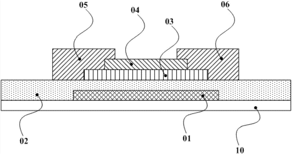
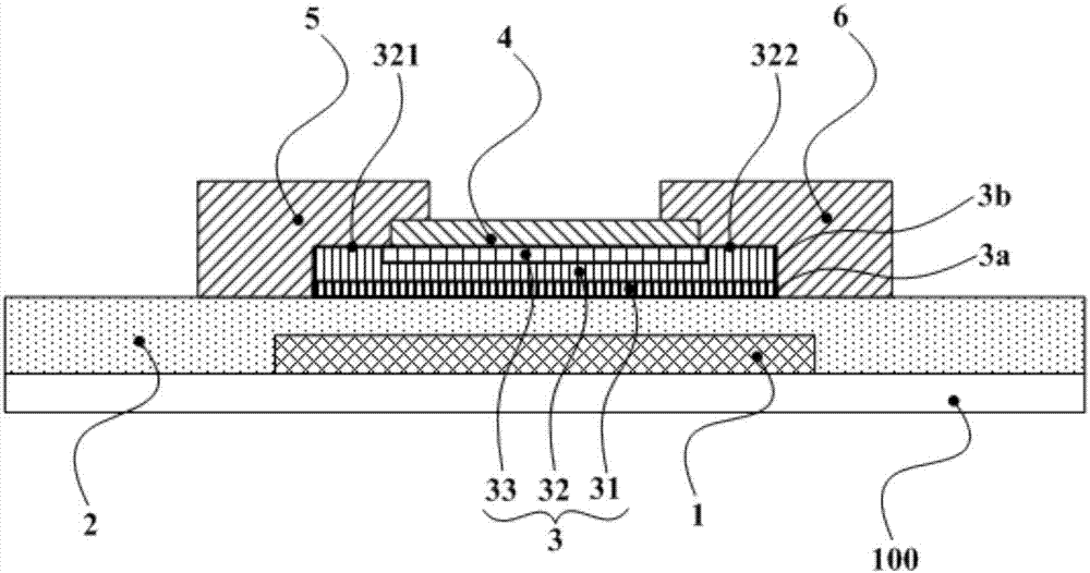
[0059] Such as figure 2 As shown, the display substrate provided by the embodiment of the present invention includes a base substrate 100 and a bottom-gate TFT disposed on the base substrate 100, and the TFT includes:

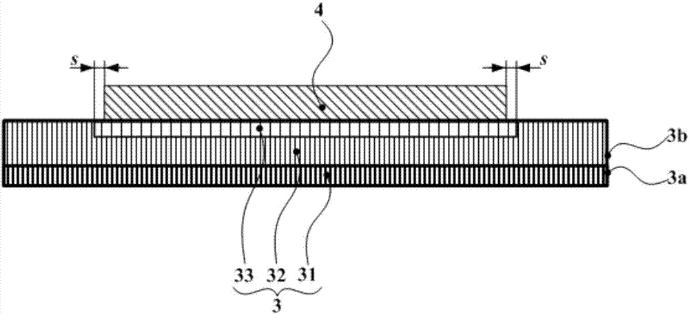
[0060] The active layer 3 includes a first concentration layer 31, a second concentration layer 32, and a third concentration layer 33 whose carrier concentration decreases sequentially along the direction away from the base substrate 100. The second concentration layer 32 includes The first connecting portion 321 connected to the pole 5 an...


PUM


Abstract

The invention discloses a display substrate, a display device and a manufacturing method of the display substrate so as to improve the performance of a thin film transistor and improve the product quality of the display device. The display substrate comprises a substrate and a bottom-gate type thin film transistor arranged on the substrate, wherein the thin film transistor comprises an active layer, an etching blocking layer, a source electrode and a drain electrode, wherein the active layer comprises a first concentration layer, a second concentration layer and a third concentration layer, the carrier concentrations of the first concentration layer, the second concentration layer and the third concentration are decreased in sequence in the direction away from the substrate, the second concentration layer comprises a first connecting part connected with the source electrode and a second connecting part connected with the drain electrode, and the third concentration layer is exposed out of the first connecting part and the second connecting part; the etching blocking layer is arranged on the side, away from the substrate, of the active layer, and does not exceed the edge of the third concentration layer; and the source electrode and the drain electrode are arranged on the side, away from the substrate, of the etching blocking layer, and are connected with the first connecting part and the second connecting part respectively.

Description

technical field [0001] The invention relates to the field of display technology, in particular to a display substrate, a display device and a method for manufacturing the display substrate. Background technique [0002] Thin Film Transistor (TFT for short) is one of the types of field effect transistors, and is mainly used in flat panel display devices. [0003] Thin Film Transistor Liquid Crystal Display (TFT-LCD) has the characteristics of small size, low power consumption, relatively low manufacturing cost and no radiation, and occupies a dominant position in the current flat panel display market. [0004] Active Matrix Organic Light Emitting Diode (AMOLED) display technology is called a new generation of display technology, which uses an independent TFT to control each light-emitting unit, and each light-emitting unit can be continuously and independently driven glow. Compared with the traditional TFT-LCD, the AMOLED display device has the advantages of fast screen swi...

Claims


Application Information

Patent Timeline
Patent Type & Authority Applications(China)
IPC IPC(8): H01L29/06H01L29/786H01L21/34
CPCH01L29/0684H01L29/66969H01L29/7869
Inventor 晏国文董正逵费强徐伟齐
Owner WUHAN TIANMA MICRO ELECTRONICS CO LTD
Why Eureka
Try Eureka