Manufacturing method of display screen, display screen and display device
A production method and technology for a display screen, applied in the field of display screen, can solve the problems such as the inability to satisfy the accuracy and reliability of punching, the difficulty of punching, etc.
- Summary
- Abstract
- Description
- Claims
- Application Information
AI Technical Summary
Problems solved by technology
Method used
Image

Examples
no. 1 example
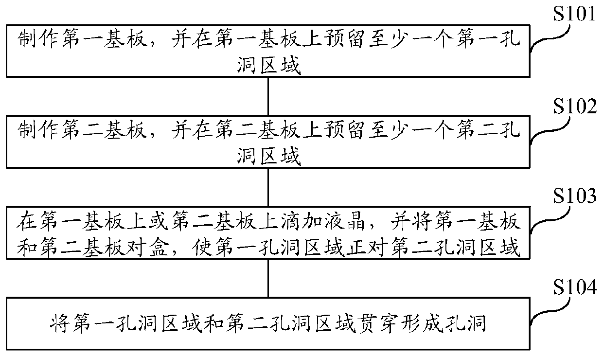
[0027] The first embodiment of the present invention discloses a display screen manufacturing method. Such as figure 1 As shown, the method includes the following steps:
[0028] Step S101: Fabricate a first substrate, and reserve at least one first hole area on the first substrate.
[0029] The first substrate may be an array substrate. The first hole area corresponds to the position of the functional element. For example, camera, receiver, HOME (main page) key and so on.
[0030] Step S102: Fabricate a second substrate, and reserve at least one second hole area on the second substrate.
[0031] The second substrate may be a color filter substrate. The second hole area corresponds to the position of the functional element. For example, camera, receiver, HOME (main page) key and so on.
[0032] Step S103: Drop liquid crystal on the first substrate or the second substrate, and align the first substrate and the second substrate so that the first hole area faces the second...
no. 2 example
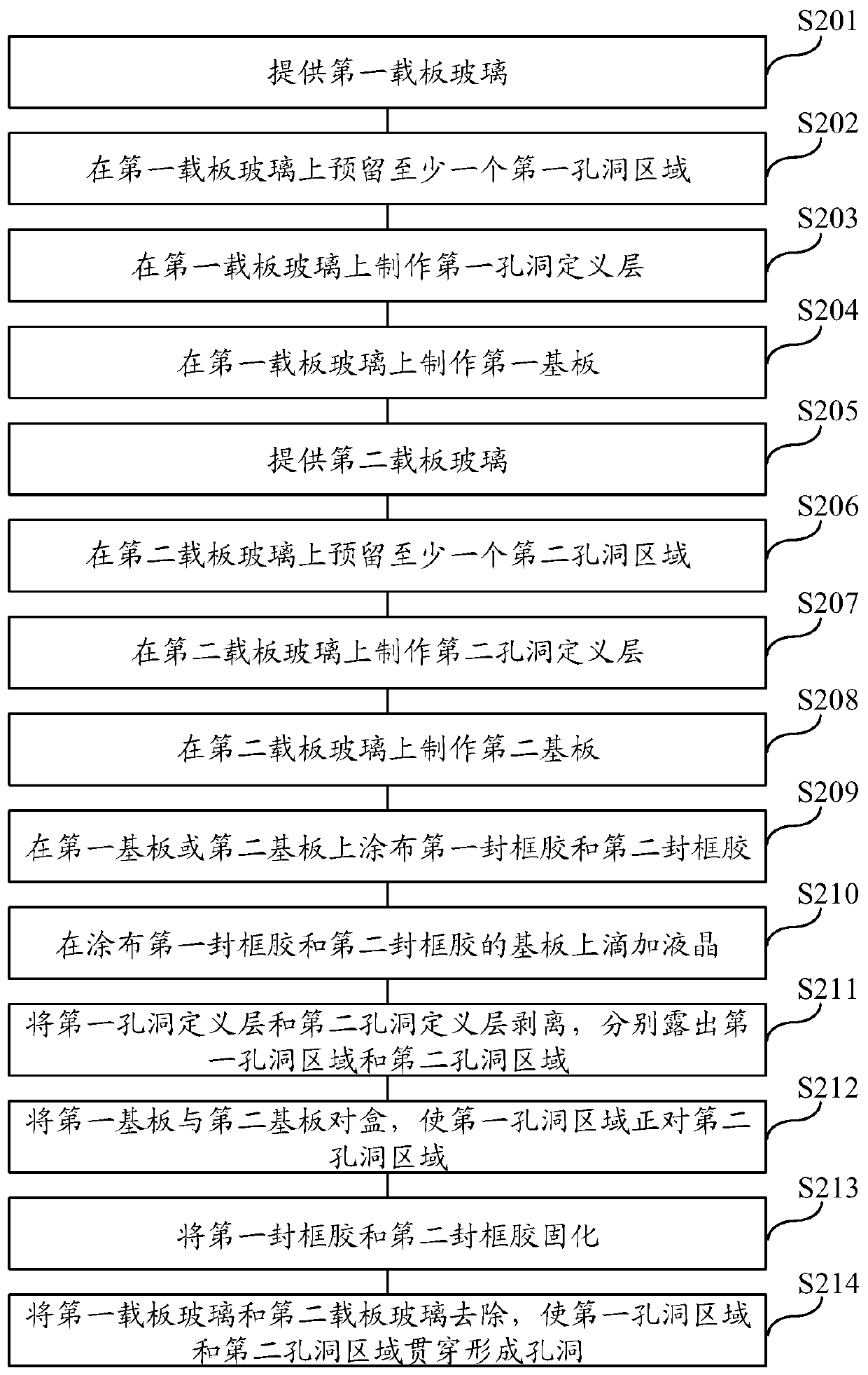
[0039] The second embodiment of the present invention discloses a display screen manufacturing method. The method for making a display screen is used for making a flexible screen. Such as figure 2 As shown, the method includes the following steps:
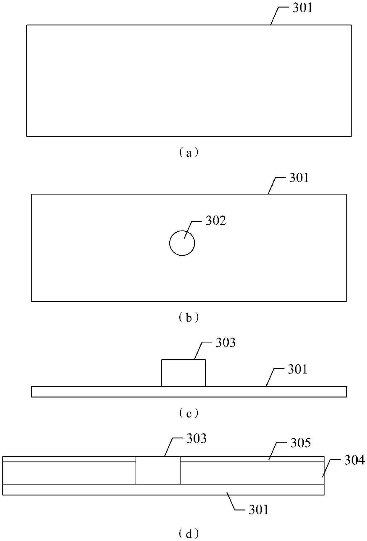
[0040] Step S201: providing a first carrier glass.
[0041] Such as image 3 As shown in (a), a first carrier glass 301 is provided.
[0042] Step S202: Reserve at least one first hole area on the first carrier glass.
[0043] Such as image 3 As shown in (b), a first hole area 302 is reserved on the first carrier glass 301 . The position of the first hole area 302 on the first carrier glass 301 corresponds to the position of the required functional module.
[0044] Step S203: making a first hole definition layer on the first carrier glass.
[0045] Such as image 3 As shown in (c), the first hole definition layer 303 is fabricated on the first carrier glass 301 such that the first hole definition layer 303 covers the fir...
no. 3 example
[0082] The third embodiment of the present invention discloses a display screen manufacturing method. The manufacturing method of the display screen is used for making a rigid screen. Such as Figure 4 As shown, the method includes the following steps:
[0083] Step S401: Reserve at least one first hole area on the first substrate.
[0084] Such as Figure 5 As shown in (a), at least one first hole area 502 is reserved on the first substrate 501 . It should be understood that the first hole region 502 formed in this step is only to reserve the position on the first substrate 501 , rather than to perforate the first substrate 501 .
[0085] Specifically, the first substrate 501 may be an array substrate, and the first substrate 501 includes a thin film transistor array 503 . The TFT array 503 is located outside the first hole area 502 .
[0086] The material of the first substrate 501 is glass.
[0087] Step S402: Reserve at least one second hole area on the second subst...
PUM
 Abstract
Description
Claims
Application Information
 - Generate Ideas
- Intellectual Property
- Life Sciences
- Materials
- Tech Scout
- Unparalleled Data Quality
- Higher Quality Content
- 60% Fewer Hallucinations
Browse by: Latest US Patents, China's latest patents, Technical Efficacy Thesaurus, Application Domain, Technology Topic, Popular Technical Reports.
© 2025 PatSnap. All rights reserved.Legal|Privacy policy|Modern Slavery Act Transparency Statement|Sitemap|About US| Contact US: help@patsnap.com