


Quick Research
Generate reliable direction feasibility study reports for your R&D in just a few steps.

Technical Q&A
Discover and master advanced knowledge NOW. Basics, ideas, possibilities, all at once.

Find Solutions
As an expert in R&D theories, this can generate solutions to your technical problems instantly.

Evaluate Feasibility
Analyze your overall solution with one click, know your potential R&D risks in advance.

Monitor Landscape
Get weekly tech updates, stay abreast of the latest tech innovations and key insights.
De-embedding method of small signal measurement
A small signal, measurement technology, applied in the direction of measuring electricity, measuring devices, measuring electrical variables, etc., can solve problems such as excessive de-embedding, and achieve the effects of convenient production, convenient calculation process, and simple structure
- Summary
- Abstract
- Description
- Claims
- Application Information
AI Technical Summary
Problems solved by technology
Method used
Image

Examples
Embodiment 1
[0035] see figure 1 As shown, a de-embedding method for small signal measurement of the present invention includes the following steps:
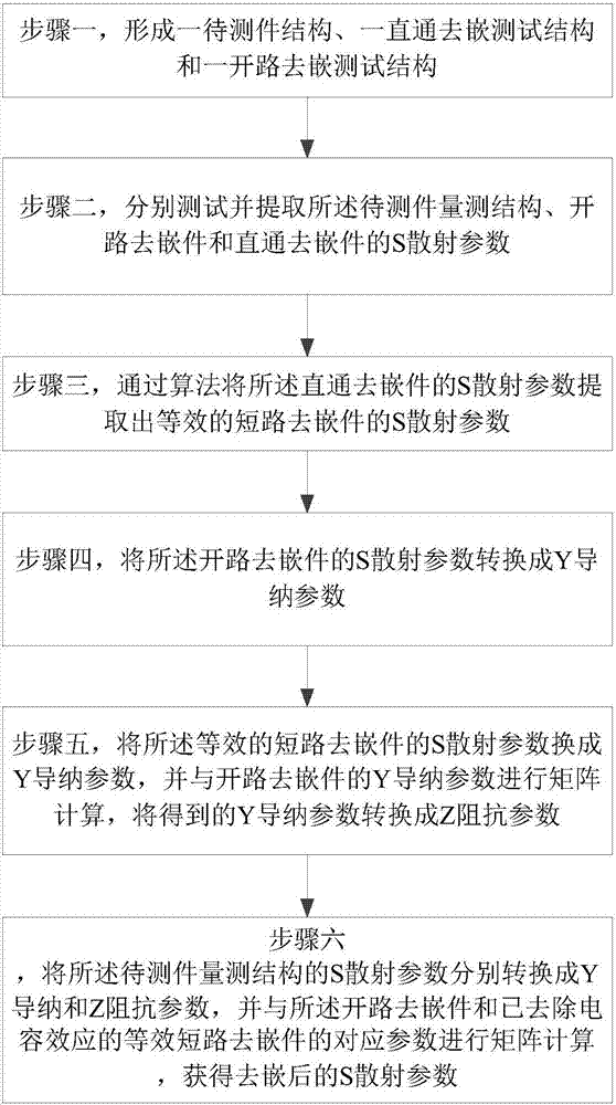
[0036] Step 1, forming a measuring structure of the DUT, a through-cut insert and an open-circuit insert. Specifically, such as figure 2 As shown, the measurement structure of the DUT includes a DUT, a signal input pad S1, a signal output pad S2, a first ground pad G1, a second ground pad G2, a third ground pad plate G3, the fourth ground pad G4, the first ground back hole V1 and the second ground back hole V2, the signal input pad S1 is connected to the input end of the DUT through the wiring metal M1, the signal The output pad S2 is connected to the output end of the DUT through the wiring metal M2, the first ground back hole V1 is connected to the ground end of the DUT under test through the wiring metal M3, and the second ground back hole V1 is connected to the ground terminal of the DUT under test through the wiring metal M3. The ho...
Embodiment 2
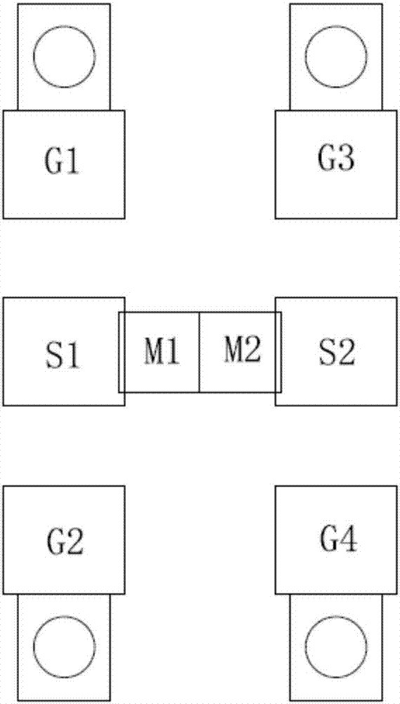
[0054] Step 1, forming a measuring structure of the DUT, a through-cut insert and an open-circuit insert. Specifically, such as figure 2 As shown, the measurement structure of the DUT includes a DUT, a signal input pad S1, a signal output pad S2, a first ground pad G1, a second ground pad G2, a third ground pad plate G3, the fourth ground pad G4, the first ground back hole V1 and the second ground back hole V2, the signal input pad S1 is connected to the input end of the DUT through the wiring metal M1, the signal The output pad S2 is connected to the output end of the DUT through the wiring metal M2, the first ground back hole V1 is connected to the ground end of the DUT under test through the wiring metal M3, and the second ground back hole V1 is connected to the ground terminal of the DUT under test through the wiring metal M3. The hole V2 is connected to the ground terminal of the DUT through the wiring metal M4. Such as image 3 As shown, the straight-through removing ...
PUM
 Abstract
Description
Claims
Application Information
 - R&D Engineer
- R&D Manager
- IP Professional
- Industry Leading Data Capabilities
- Powerful AI technology
- Patent DNA Extraction
Browse by: Latest US Patents, China's latest patents, Technical Efficacy Thesaurus, Application Domain, Technology Topic, Popular Technical Reports.
© 2024 PatSnap. All rights reserved.Legal|Privacy policy|Modern Slavery Act Transparency Statement|Sitemap|About US| Contact US: help@patsnap.com