Probe

A technology of probes and main parts, which is applied in the direction of printed circuit testing, instruments, measuring devices, etc., and can solve the problems of miniaturization of circuit boards, high-density obstacles, etc.

Active Publication Date: 2017-09-08
MURATA MFG CO LTD
View PDF8 Cites 12 Cited by
  • Summary
  • Abstract
  • Description
  • Claims
  • Application Information

AI Technical Summary

Problems solved by technology

That is, the inspection of circuit boards using conventional probes has become an obstacle to the miniaturization and high density of the circuit boards.

Method used


Image

  • Probe
  • Probe
  • Probe

Examples


Embodiment Construction

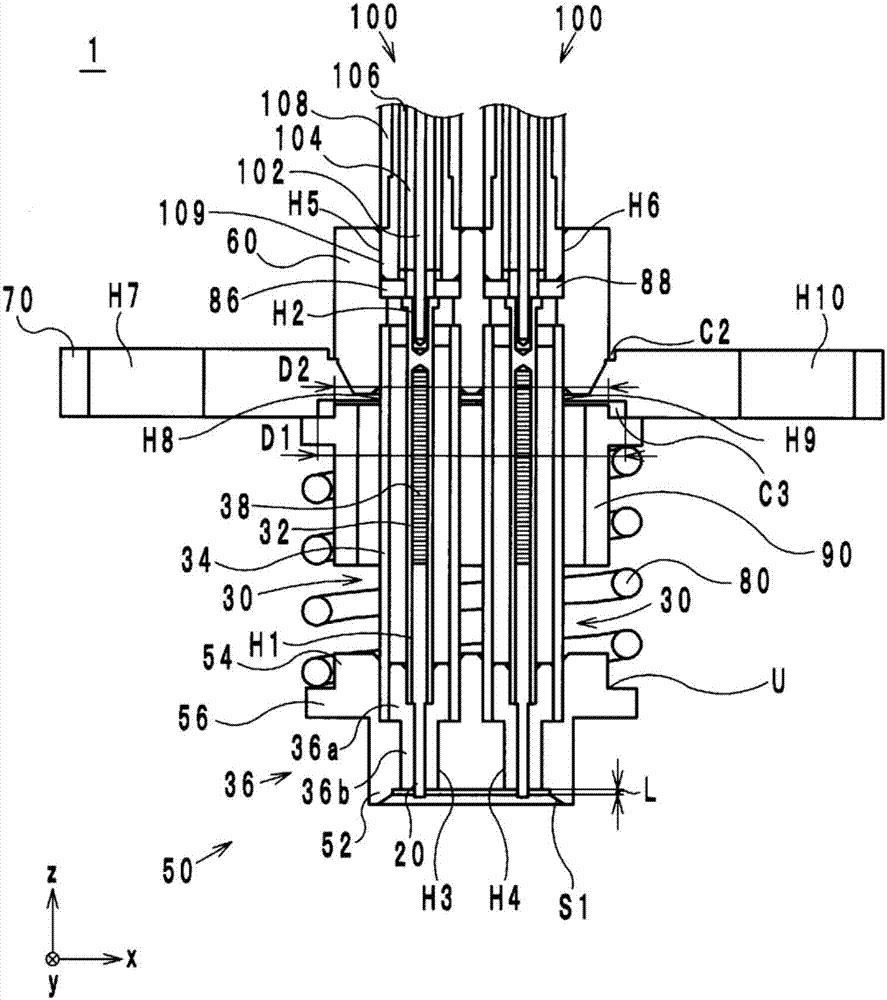
[0020] A probe 1 as an example will be described with reference to the drawings. Hereinafter, the direction from the tip of the probe 1 toward the cable is defined as the z-axis direction. In addition, the direction in which the central conductors included in the probe 1 is defined as the x-axis direction. And, the direction perpendicular to the x-axis and the z-axis is defined as the y-axis direction. In addition, the x-axis, y-axis, and z-axis are orthogonal to each other. In addition, the surface on the positive side in the z-axis direction is referred to as an upper surface, and the surface on the negative side in the z-axis direction is referred to as a lower surface. In addition, a surface parallel to the z-axis direction is called a side surface.

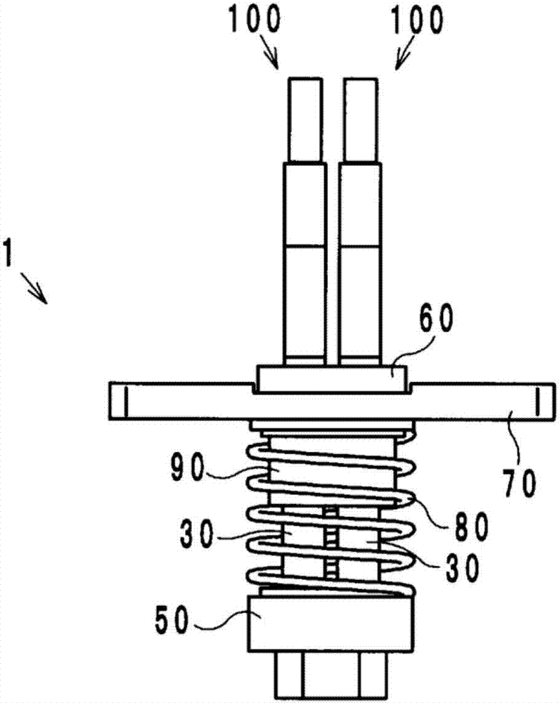
[0021] (For a rough structure of the probe, refer to figure 1 )

[0022] The probe 1 is a probe capable of simultaneously measuring electrical signals emitted from two terminals provided on a circuit board. Therefore, i...


PUM


Abstract

The purpose of the present invention is to provide a probe whereby increased density of electronic components, being the measurement target, is possible on a circuit board. The probe (1) is capable of simultaneously measuring a plurality of locations. The probe (1) comprises: a plurality of main body sections (30) including central conductors (20) that come in contact with a connector (300); and a first member (50) that bundles the plurality of main body sections (30). A recessed section (C1), having the tips of the plurality of central conductors (20) protruding from the bottom surface thereof, is provided in the first member (50). The recessed section (C1) has a sloping surface (S1) that spreads from said bottom surface towards an opening.

Description

technical field [0001] The present invention relates to probes used for measurement of electronic components. Background technique [0002] In recent years, communication terminals that can handle multiple frequencies are becoming mainstream. Such a communication terminal has a plurality of RF circuits, and each RF circuit is connected to an antenna module. In addition, each RF circuit has a connector for connection to the antenna module. Here, in checking the operation of the RF circuit of the communication terminal, a plurality of RF circuits are operated simultaneously, and the operation is confirmed by pressing a probe against each connector. Furthermore, the probe described in Patent Document 1 (hereinafter, referred to as a conventional probe) is known as a probe used for checking the operation of the RF circuit and the like. [0003] However, as described above, current communication terminals have a plurality of RF circuits, and have connectors for connection with...

Claims


Application Information

Patent Timeline
Patent Type & Authority Applications(China)
IPC IPC(8): G01R1/073G01R1/067G01R31/26
CPCG01R1/0408G01R1/06772G01R31/2808G01R1/067G01R1/07314G01R31/2801G01R31/2822
Inventor 由井孝欣
Owner MURATA MFG CO LTD
Why Eureka
Try Eureka