An organic light emitting diode curved surface display panel, display device and manufacturing method
A light-emitting diode and curved surface display technology, which is applied to organic light-emitting devices, organic light-emitting device structures, organic semiconductor devices, etc., can solve the problems of single viewing angle, internal temperature rise, inconsistent colors, etc., to overcome the single viewing angle and prolong the practical life , to ensure the effect of connection stability
- Summary
- Abstract
- Description
- Claims
- Application Information
AI Technical Summary
Problems solved by technology
Method used
Image
Examples
Embodiment 1
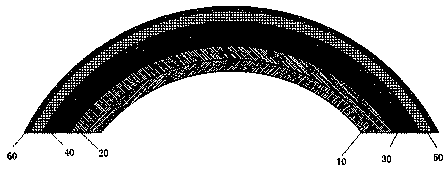
[0047] like figure 1As shown, this embodiment provides an organic light emitting diode curved display panel, including a glass substrate 50, an anode layer 40, a conductive layer 30, a light emitting layer 20 and a cathode layer 10, a glass substrate 50, an anode layer 40, a conductive layer 30, and a light emitting Both the layer 20 and the cathode layer 10 are arc-shaped and coaxially distributed, along the axis from the inside to the outside are the cathode layer 10, the light emitting layer 20, the conductive layer 30, the anode layer 40 and the glass substrate 50; the outside of the glass substrate 50 An anti-reflection layer 60 is provided on the surface, the anti-reflection layer 60 is in the shape of an arc plate, and the anti-reflection layer 60 is coaxially distributed with the glass substrate 50 .
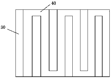
[0048] When the display panel is working, an external power supply applies a voltage between the anode layer 40 and the cathode layer 10, and electrons flow from the cat...
Embodiment 2
[0052] This embodiment provides an OLED curved display panel, including a glass substrate 50, an anode layer 40, a conductive layer 30, a light emitting layer 20 and a cathode layer 10, a glass substrate 50, an anode layer 40, a conductive layer 30, a light emitting layer 20 and The cathode layer 10 is arc-shaped and coaxially distributed, along the axis from the inside to the outside are the cathode layer 10, the light emitting layer 20, the conductive layer 30, the anode layer 40 and the glass substrate 50; the light emitting layer 20 is the inner surface area Greater than the outer surface area of the cathode layer 10, the outer surface area of the luminescent layer 20 is greater than the inner surface area of the conductive layer 30, and the luminescent layer 20 can rotate relative to the conductive layer 30 and the cathode layer 10 with the axis as the axis.
[0053] The inner surface area of the arc-shaped luminescent layer 20 is greater than the outer surface are...
Embodiment 3
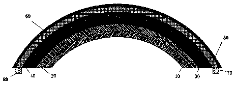
[0055] like figure 2 As shown, this embodiment provides an organic light emitting diode curved display panel, including a glass substrate 50, an anode layer 40, a conductive layer 30, a light emitting layer 20 and a cathode layer 10, a glass substrate 50, an anode layer 40, a conductive layer 30, and a light emitting Both the layer 20 and the cathode layer 10 are arc-shaped and coaxially distributed, along the axis from the inside to the outside are the cathode layer 10, the light emitting layer 20, the conductive layer 30, the anode layer 40 and the glass substrate 50; the light emitting layer 20 is The inner surface area is greater than the outer surface area of the cathode layer 10, the outer surface area of the luminescent layer 20 is greater than the inner surface area of the conductive layer 30, the luminescent layer 20 can be rotated relative to the conductive layer 30 and the cathode layer 10 on the axis; the side of the glass substrate 50 is provided with a ligh...
PUM
 Abstract
Description
Claims
Application Information
 - R&D
- Intellectual Property
- Life Sciences
- Materials
- Tech Scout
- Unparalleled Data Quality
- Higher Quality Content
- 60% Fewer Hallucinations
Browse by: Latest US Patents, China's latest patents, Technical Efficacy Thesaurus, Application Domain, Technology Topic, Popular Technical Reports.
© 2025 PatSnap. All rights reserved.Legal|Privacy policy|Modern Slavery Act Transparency Statement|Sitemap|About US| Contact US: help@patsnap.com


