Planar optical element absolute surface shape detection device

A technology of optical components and detection devices, applied in the direction of using optical devices, measuring devices, instruments, etc., can solve the problems of losing medium and high frequency information of the wave front, affecting the accuracy of absolute detection and measurement, and incomplete plane shape information, etc.

Active Publication Date: 2017-08-11
SHANGHAI INST OF OPTICS & FINE MECHANICS CHINESE ACAD OF SCI
View PDF5 Cites 11 Cited by
  • Summary
  • Abstract
  • Description
  • Claims
  • Application Information

AI Technical Summary

Problems solved by technology

[0003] At this stage, interferometer detection is all relative measurement, and the accuracy of interferometric detection is limited by the reference mirror shape of the interferometer itself (PV value is generally better than 0.1λ), especially when the surface quality PV of the detection element is better than 0.1λ or even higher At this time, the accuracy of the measurement results cannot be judged

Method used


Image

  • Planar optical element absolute surface shape detection device
  • Planar optical element absolute surface shape detection device
  • Planar optical element absolute surface shape detection device

Examples


Embodiment Construction

[0048] The present invention will be further described below in conjunction with embodiment, but should not limit the transformation range of the present invention with this.

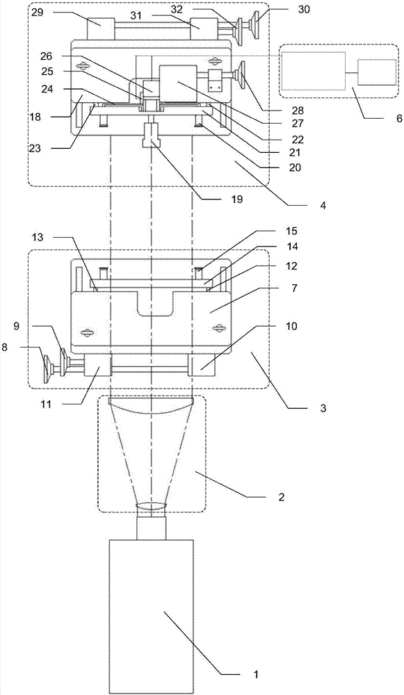
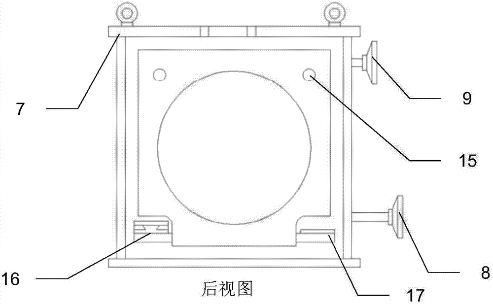
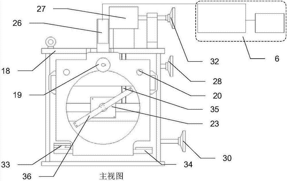
[0049] see first figure 1 , figure 2 , image 3 , Figure 4 , figure 1 It is a top view of the absolute surface shape detection device of the planar optical element of the present invention; figure 2 is the rear view of the transmission mirror two-dimensional adjustment system; image 3 Front view of the mirror four-dimensional adjustment system; Figure 4 It is the front view of the planar optical element fixture; as can be seen from the figure, the composition of the best embodiment of the absolute surface shape detection device of the planar optical element of the present invention includes a laser interferometer 1, a beam expander collimation system 2, and a transmission mirror two-dimensional adjustment system 3 , Mirror four-dimensional adjustment system 4, 3 sets of planar optical eleme...


PUM


Abstract

The invention discloses a planar optical element absolute surface shape detection device. The planar optical element absolute surface shape detection device comprises a laser interferometer, a beam expanding collimation system, a transmitting mirror two-dimensional adjusting system, a reflector four-dimensional adjusting system, three planar optical element clamps, three planar optical elements, and a reflector rotation electrical appliance control system. The planar optical element absolute surface shape detection device is advantageous in that the planar optical element absolute surface shape detection is realized, and an object of improving detection precision is realized, and then a processing level is evaluated in a marked way, and therefore guiding significance is provided for further improvement of processing precision.

Description

technical field [0001] The invention relates to high-precision detection of high-precision planar optical elements, in particular to an absolute surface shape detection device for planar optical elements. It can realize the absolute surface shape detection of the full aperture of the planar component, improve the detection accuracy, and have a more iconic quantitative processing level, and realize the guiding significance for the further breakthrough of the processing accuracy. Background technique [0002] At present, optical components have higher and higher requirements for detection level, especially in projection lithography exposure optical system, the RMS value of component surface shape is required to reach nanometer or even sub-nanometer level, which is a very high challenge for optical detection level. At present, interferometry is the most effective method for measuring high-precision optical planes. The commonly used surface shape detection methods for optical c...

Claims


Application Information

Patent Timeline
IPC IPC(8): G01B11/24
CPCG01B11/2441
Inventor 刘世杰白云波周游张志刚吴福林王圣浩鲁棋王微微邵建达
Owner SHANGHAI INST OF OPTICS & FINE MECHANICS CHINESE ACAD OF SCI
Why Eureka
Try Eureka