
Solid state hard disk device with warning device and relevant solid state hard disk control circuit

A solid-state hard disk and warning device technology, applied in the direction of alarm, static memory, read-only memory, etc., can solve the problems of time-consuming, user trouble, interference with the normal operation of the solid-state hard disk control circuit, etc., to avoid incorrect operation, reduce damaged effect

Inactive Publication Date: 2017-08-04
RAYMX MICROELECTRONICS CORP
View PDF7 Cites 2 Cited by
  • Summary
  • Abstract
  • Description
  • Claims
  • Application Information

AI Technical Summary

Problems solved by technology

[0003] As we all know, it takes a lot of time for the solid state drive control circuit to build and update these tables
In addition, during the process of establishing and updating these tables by the control circuit of the solid-state hard disk, it may be temporarily unable to respond to the access command or query command of the main control device, thus causing confusion or confusion to the user
[0004] When the solid-state hard disk control circuit cannot respond to the command of the main control device, if the user performs incorrect operations on the solid-state hard disk device, for example, turning off the power of the solid-state hard disk device or restarting the entire system, etc., it will interfere with the solid-state hard disk. The normal operation of the control circuit will cause damage to the solid-state hard disk device, and even cause the data in the solid-state hard disk device to be unreadable

Method used


Image

  • Solid state hard disk device with warning device and relevant solid state hard disk control circuit

Examples


Embodiment Construction

[0025] The embodiments of the present invention will be described below in conjunction with related drawings. In the drawings, the same reference numerals indicate the same or similar components or method flows.

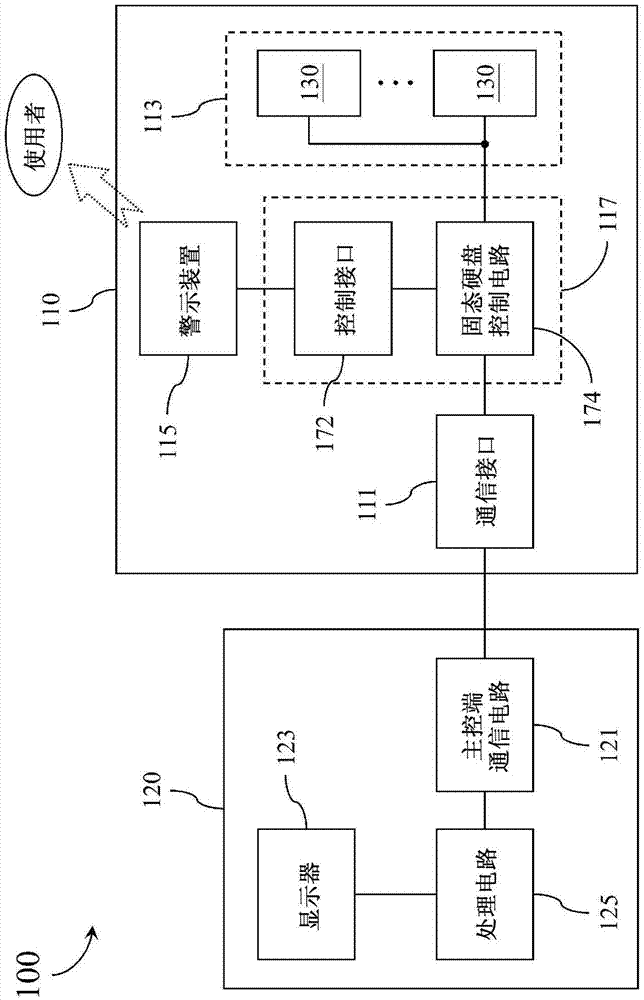
[0026] figure 1 It is a simplified functional block diagram of the solid state disk access system 100 according to an embodiment of the present invention. The solid state disk access system 100 includes a solid state drive device (SSD device) 110 and a host device 120.

[0027] in figure 1 In the embodiment, the solid state drive device 110 includes a communication interface 111, a solid state drive (SSD) 113, a warning device 115, and a solid state drive control circuit (SSD controlling circuit) 117. The main control device 120 includes a host-end communication circuit 121, a display 123, and a processing circuit 125.

[0028] In the solid state hard disk device 110, the communication interface 111 is configured to perform data communication with the main control termi...


PUM


Abstract

The invention provides a solid state hard disk device with a warning device and a relevant solid state hard disk control circuit. The solid state hard disk device comprises a communication interface, a solid state hard disk and the solid state hard disk control circuit, wherein the communication interface performs data communication with a main control device; the solid state hard disk comprises one or a plurality of flash memory arrays; the solid state hard disk control circuit comprises a control interface and a flash memory control circuit. After the solid state hard disk control circuit is electrified, if the flash memory control circuit cannot perform data communication with the main control device through the communication interface, or the flash memory control circuit detects the condition that present events occur in the solid state hard disk, the flash memory control circuit can control the warning device to generate preset sound or preset light rays or the combination of the preset sound and the light rays through the control interface so as to send out warning to a user of the solid state hard disk device.

Description

Technical field [0001] The present invention relates to a solid state drive, especially a solid state drive device with a built-in warning device and a related solid state drive control circuit. Background technique [0002] Due to the fast access speed of solid state drive (SSD) devices, more and more traditional hard disk devices are replaced by solid state drive devices. Unlike traditional hard disk devices, solid-state hard disk devices need to rely on the solid-state hard disk control circuit to establish and update the address mapping table and other management tables corresponding to the data stored in the solid-state hard disk device in order to enable the main control device to pass the solid state drive. The hard disk control circuit accesses the solid state hard disk device. [0003] As we all know, it takes a lot of time for the SSD control circuit to build and update these tables. In addition, during the process of establishing and updating these tables by the solid ...

Claims


Application Information

Patent Timeline
Patent Type & Authority Applications(China)
IPC IPC(8): G11C16/22G08B21/18
CPCG11C16/22G08B21/18
Inventor 陈彦仲陈政宇简志清
Owner RAYMX MICROELECTRONICS CORP
Learn More