Nand-flash storage array Mapping management method
A storage array and management method technology, applied in the field of high-speed and large-capacity storage, can solve the problems of very strict storage device capacity and read/write rate, time-consuming, etc., and achieve the goals of reducing the amount of erasure, simplifying the update speed, and improving the update speed Effect
- Summary
- Abstract
- Description
- Claims
- Application Information
AI Technical Summary
Problems solved by technology
Method used
Image
Examples
Embodiment
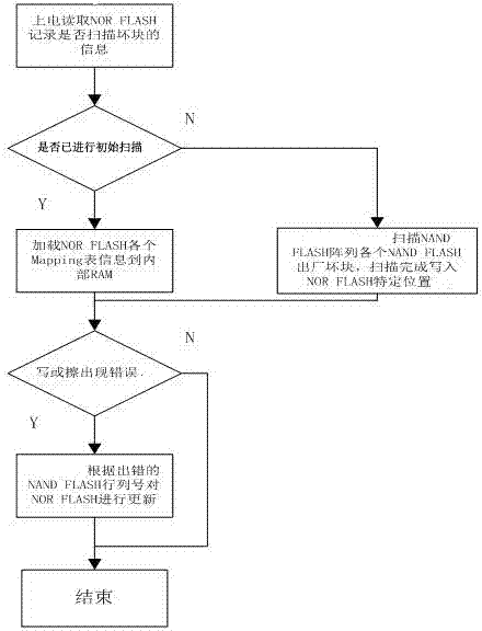
[0017] The Nand-flash storage array Mapping management method described in this embodiment, according to the wrong NAND FLASH row, column position to erase and update the specific position of NOR FLASH, it mainly includes the following steps: initially scan bad blocks, power-on loading and update Bad block three steps.
[0018] The step of initially scanning for bad blocks mainly refers to reading the initial bad block information in each NAND FLASH in the NAND FLASH array through parallel pipeline to form an initial Mapping table.
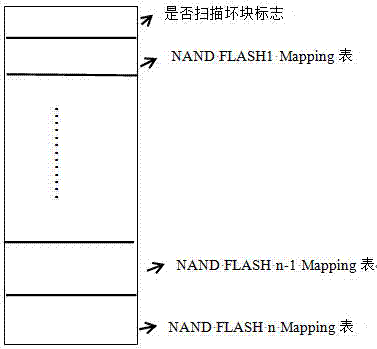
[0019] In the step of initial scanning of bad blocks, the address data of each NAND FLASH in the NAND FLASH array that records the factory bad block information is sequentially read to determine whether it is a factory bad block, and an initial Mapping table is formed, which is stored in different locations of NOR FLASH.
[0020] The step of power-on loading mainly means that when the system is powered on, the Mapping table information in the NOR ...
PUM
 Abstract
Description
Claims
Application Information
 - R&D
- Intellectual Property
- Life Sciences
- Materials
- Tech Scout
- Unparalleled Data Quality
- Higher Quality Content
- 60% Fewer Hallucinations
Browse by: Latest US Patents, China's latest patents, Technical Efficacy Thesaurus, Application Domain, Technology Topic, Popular Technical Reports.
© 2025 PatSnap. All rights reserved.Legal|Privacy policy|Modern Slavery Act Transparency Statement|Sitemap|About US| Contact US: help@patsnap.com


