Apparatus and method for producing lateral HEMT

A lateral and buffer layer technology, used in semiconductor/solid-state device manufacturing, semiconductor devices, electrical components, etc., can solve problems such as poor heat dissipation and poor thermal coupling of components, and achieve higher breakdown voltage, reduced leakage current, and improved Effects of off-characteristics and on-characteristics

Active Publication Date: 2017-07-28
ROBERT BOSCH GMBH
View PDF13 Cites 0 Cited by
  • Summary
  • Abstract
  • Description
  • Claims
  • Application Information

AI Technical Summary

Problems solved by technology

A disadvantage here is that the thermal coupling of the rear side of the semiconductor to, for example, a printed circuit board or a sheet metal is worse, since a partially removed substrate is arranged between the heat-conducting coupling body and the semiconductor, which makes the heat dissipation of the component worse.

Method used


Image

  • Apparatus and method for producing lateral HEMT
  • Apparatus and method for producing lateral HEMT
  • Apparatus and method for producing lateral HEMT

Examples


Embodiment Construction

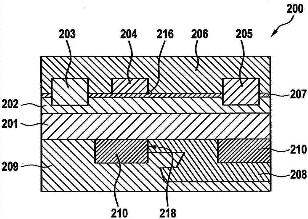
[0036] figure 1 A device 100 with a transverse HEMT according to the invention is shown. In this case, the lateral HEMT has a buffer layer 101 comprising the first semiconductor material. Arranged on the buffer layer 101 is a further semiconductor layer 102 which comprises a second semiconductor material, wherein the second semiconductor material has a different electrode mobility than the first semiconductor material. In other words, a heterostructure is formed because the first semiconductor material and the second semiconductor material are different. A first electrode 103 , a gate 104 and a second electrode 105 are arranged on the further semiconductor layer 102 . Optionally, a gate dielectric layer 107 is disposed on the other semiconductor layer 102 . An insulating protective layer is arranged on the first electrode 103 , the grid 104 and the second electrode 105 , which protects the electrodes 103 , 104 and 105 against mechanical influences. A first field plate 109 ...


PUM


Abstract

An apparatus (100, 200, 300, 400) including a lateral HEMT is provided. The lateral HEMT comprises at least one buffer layer (101, 201, 301, 401) on which another semiconductor layer (102, 202, 302, 402) is arranged. A first electrode (103, 203, 303, 403), a grid electrode (104, 204, 304, 404) and a second electrode (105, 205, 305, 140) are arranged on the second semiconductor layer (102, 202, 302, 402). The apparatus is characterized in that a first field plate (109, 209, 309, 409) is arranged below the buffer layer (101, 201, 301, 401), and the first field plate (109, 209, 309, 409) is at least partially abutted against the buffer layer (101, 201, 301, 401).

Description

technical field [0001] The present invention relates to an apparatus and a method for manufacturing a lateral HEMT. Background technique [0002] HEMT (High-electron-mobility Transistoren) through, for example, aluminum gallium nitride / gallium nitride (AiGaN / GaN) or indium gallium nitride (InGaN) or aluminum nitride / gallium nitride (AlN / GaN) Heterostructures are deposited by deposition on substrates such as sapphire, silicon carbide (SiC) or silicon (Si). In this case, the deposition of GaN on Si results in a high load in the growing GaN layer due to the large lattice mismatch between Si and GaN. Furthermore, silicon is mechanically unstable at the typical temperatures for GaN growth, typically in the range of 1000 to 1200° C. In order to reduce this load, doped silicon having a face-centered cubic lattice structure with {111} planes is used for the deposition of GaN for the production of such HEMT transistors. A disadvantage here is that high substrate leakage currents o...

Claims


Application Information

Patent Timeline
Patent Type & Authority Applications(China)
IPC IPC(8): H01L29/778H01L29/40H01L21/335
CPCH01L29/402H01L29/404H01L29/66462H01L29/7786H01L29/4175H01L29/2003
Inventor S·A·尧斯S·施魏格尔
Owner ROBERT BOSCH GMBH
Why Eureka
Try Eureka