Optical brightness enhancement structure and manufacturing method thereof

A production method and optical technology, applied in the directions of optics, optical components, optical components, etc., can solve the problems of complicated production process of brightness enhancement film, and achieve the effect of easy production and molding, and simplified production process.

Active Publication Date: 2017-07-07
BOE TECH GRP CO LTD
View PDF5 Cites 2 Cited by
  • Summary
  • Abstract
  • Description
  • Claims
  • Application Information

AI Technical Summary

Problems solved by technology

[0004] However, no matter which of the above-mentioned methods is used to make the brightness enhancement film, due to the high requirements for the shape of the condenser prism in the brightness enhancement film, the etching or processing of the condenser prism needs to have high precision, which inevitably requires multiple inspections and corrections The etching angle or processing angle of the condensing prisms, as well as multiple adjustments to align the orientation of each condensing prism, complicate the production process of the brightness enhancement film.

Method used


Image

  • Optical brightness enhancement structure and manufacturing method thereof
  • Optical brightness enhancement structure and manufacturing method thereof
  • Optical brightness enhancement structure and manufacturing method thereof

Examples


Embodiment Construction

[0023] In order to further illustrate the optical brightness enhancement structure provided by the embodiments of the present invention and the manufacturing method thereof, a detailed description will be given below in conjunction with the accompanying drawings.

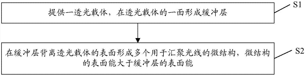
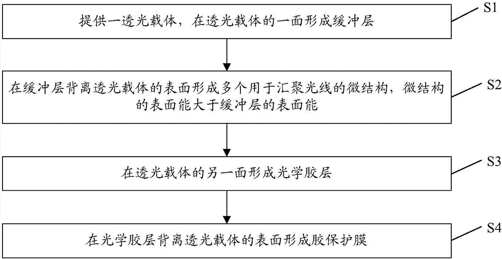
[0024] refer to figure 2 , the manufacturing method of the optical brightness enhancement structure provided by the embodiment of the present invention includes:

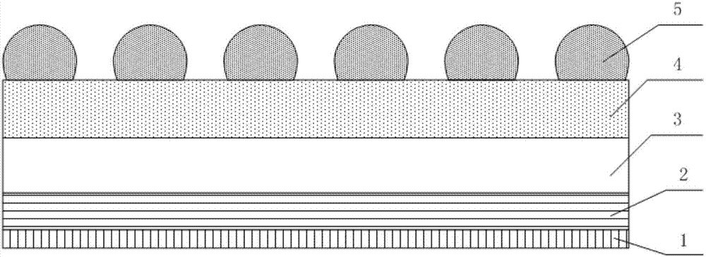
[0025] S1, providing a light-transmitting carrier, forming a buffer layer on one side of the light-transmitting carrier;

[0026] S2, forming a plurality of microstructures for converging light on the surface of the buffer layer away from the light-transmitting carrier; the surface energy of the microstructures is greater than the surface energy of the buffer layer.

[0027] During specific implementation, the material with less surface energy is selected to form a buffer layer on one side of the light-transmitting carrier, and the material with larger ...


PUM

PropertyMeasurementUnit
thicknessaaaaaaaaaa
thicknessaaaaaaaaaa
thicknessaaaaaaaaaa

Abstract

The invention discloses an optical brightness enhancement structure and a manufacturing method thereof, relates to the display technical field and is to simplify manufacturing process of the optical brightness enhancement structure. The optical brightness enhancement structure comprises a light-transmitting carrier and a buffer layer formed on one surface of the light-transmitting carrier. The buffer layer is provided with a plurality of microstructures for gathering light rays, wherein the surface energy of each microstructure is larger than that of the buffer layer. The manufacturing method of the optical brightness enhancement structure comprises the following steps: providing the light-transmitting carrier and forming the buffer layer on one surface of the light-transmitting carrier; and forming the plurality of microstructures for gathering light rays on the surface, away from the light-transmitting carrier, of the buffer layer, wherein the surface energy of each microstructure is larger than that of the buffer layer. The optical brightness enhancement structure and the manufacturing method thereof are used for a surface light-emitting illuminating device or a display device.

Description

technical field [0001] The invention relates to the field of display technology, in particular to an optical brightness enhancement structure and a manufacturing method thereof. Background technique [0002] Brightness Enhancement Film (BEF for short), also called brightness enhancement film or prism sheet, is widely used in backlight modules because it can gather light emitted by a light source and improve light output efficiency of the light source. [0003] At present, the traditional brightness enhancement film is composed of a plurality of identical elongated light-concentrating prisms regularly arranged in a certain direction, and the cross-section of each light-concentrating prism is an isosceles triangle. In the process of making this traditional brightness-enhancing film, it is necessary to etch the corresponding light-concentrating prisms on the substrate one by one according to the set prism angle and prism length to form the brightness-enhancing film; or, accordi...

Claims


Application Information

Patent Timeline
Patent Type & Authority Applications(China)
IPC IPC(8): G02B5/02
CPCG02B5/0205G02B5/0268G02B5/0226G02B5/0278B29D11/0074B29D11/00298G02B5/0215
Inventor 高昕伟
Owner BOE TECH GRP CO LTD
Why Eureka
Try Eureka