Pixel circuit and driving method thereof, and active-matrix organic light emission display device
A pixel circuit, organic technology, applied to circuits, electrical components, static indicators, etc., can solve the problems of image quality deterioration of active matrix organic light-emitting display devices, flickering of organic light-emitting diodes (OLEDs), and uneven display brightness, etc. Achieve the effect of improving display brightness uniformity, avoiding threshold voltage deviation, and preventing hysteresis effect
- Summary
- Abstract
- Description
- Claims
- Application Information
AI Technical Summary
Problems solved by technology
Method used
Image
Examples
no. 1 example
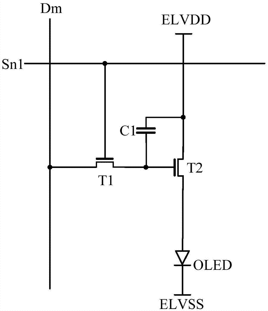
[0024] figure 2 It is a specific circuit diagram of the pixel circuit provided by the first embodiment of the present invention. Please refer to figure 2 , the pixel circuit includes: thin film transistor T1 (first thin film transistor), thin film transistor T2 (second thin film transistor), thin film transistor T3 (third thin film transistor), thin film transistor T4 (fourth thin film transistor), thin film transistor T5 (fifth thin film transistor), thin film transistor T6 (sixth thin film transistor), capacitor C, organic light emitting diode OLED1.
[0025] Specifically, the gate of the thin film transistor T1 is electrically connected to the light emission control line Em, the first end of the thin film transistor T1 is electrically connected to the first power supply Vdd, and the second end of the thin film transistor T1 is electrically connected to the first node b. The gate of the thin film transistor T2 is electrically connected to the light emission control line ...
no. 2 example
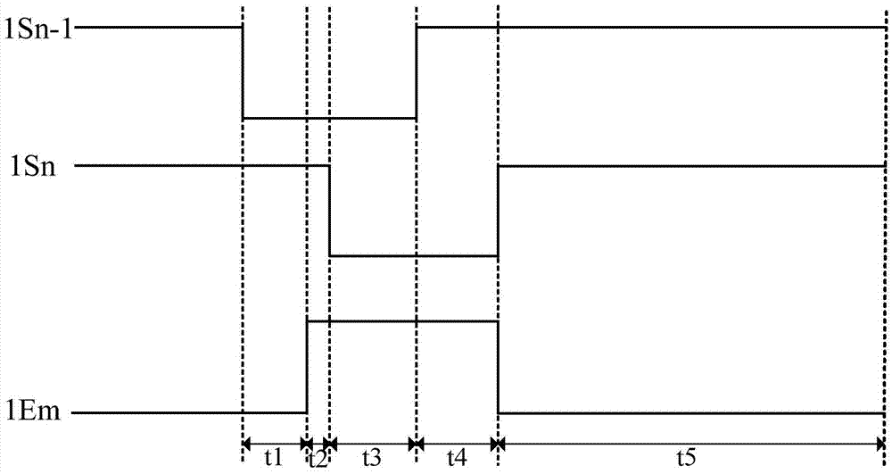
[0045] Figure 5 It is a flow chart of the steps of the driving method for driving the pixel circuit in the first embodiment provided by the second embodiment of the present invention. Please refer to Figure 3 to Figure 5The driving method of the pixel circuit in this embodiment may include the following steps: Steps 501-504, preferably, Step 505 may also be included.
[0046] The scanning cycle includes a first time period t1, a second time period t2, a third time period t3, and a fourth time period t4. Preferably, it may also include a fifth time period t5 (also called a light-emitting period):
[0047] Step 501, in the first time period t1, control the scanning signal provided by the second scanning line Sn-1 and the control signal provided by the light emission control line Em to be low level, and control the scanning signal provided by the first scanning line Sn to be high level , the transistors T5 and T6 are turned on, the potential of the anode of the organic light ...
PUM
 Abstract
Description
Claims
Application Information
 - R&D
- Intellectual Property
- Life Sciences
- Materials
- Tech Scout
- Unparalleled Data Quality
- Higher Quality Content
- 60% Fewer Hallucinations
Browse by: Latest US Patents, China's latest patents, Technical Efficacy Thesaurus, Application Domain, Technology Topic, Popular Technical Reports.
© 2025 PatSnap. All rights reserved.Legal|Privacy policy|Modern Slavery Act Transparency Statement|Sitemap|About US| Contact US: help@patsnap.com


