Method for removing solder from wafer surface

A wafer and solder technology, which is used in the field of removing solder on the surface of wafers, can solve the problem of difficulty in ensuring the uniformity of sample grinding, and achieve the effect of a simple removal process.

Inactive Publication Date: 2017-05-31
WUHAN XINXIN SEMICON MFG CO LTD
View PDF4 Cites 5 Cited by
  • Summary
  • Abstract
  • Description
  • Claims
  • Application Information

AI Technical Summary

Problems solved by technology

At present, most laboratories use mechanical grinding to remove solder, but due to the inconsistency between solder and surrounding materials, it is difficult to ensure the uniformity of sample grinding

Method used


Image

  • Method for removing solder from wafer surface
  • Method for removing solder from wafer surface

Examples


Embodiment Construction

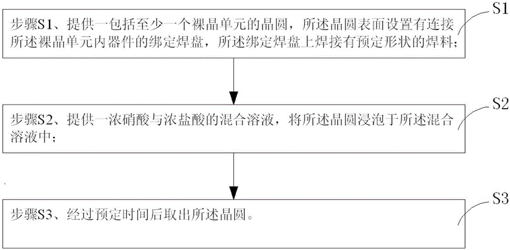
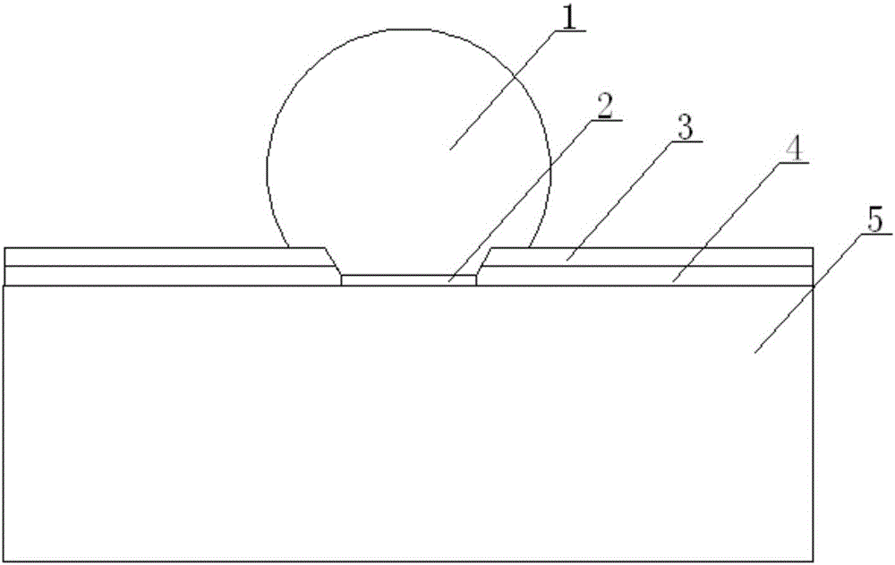
[0026] In the following description, numerous specific details are given in order to provide a more thorough understanding of the present invention. Of course, the present invention can also have other embodiments besides these detailed descriptions.

[0027] The invention proposes a method for removing the solder on the surface of the wafer, the removal process is simple, and the method for removing the solder on the surface of the wafer can be completely removed without affecting the performance of the chip and the observation effect.

[0028] The present invention will be further described below in conjunction with the accompanying drawings and specific embodiments. Obviously, the described examples are only some examples of the present invention, not all examples. Based on the examples summarized in the present invention, all examples obtained by persons of ordinary skill in the art without making creative efforts belong to the protection scope of the present invention.

...


PUM


Abstract

The present invention relates to the field of semiconductors and especially relates to a method for removing a solder from a wafer surface. The method comprises the steps of (S1) providing a wafer comprising at least one bare wafer unit, wherein the surface of the wafer is provided with a binding pad connected to a device in the bare wafer unit, and the solder with a predetermined shape is welded to the binding pad, (S2) providing a mixed solution of concentrated nitric acid and concentrated hydrochloric acid, and placing the wafer into the mixed solution, and (S3) taking the wafer out after a predetermined period of time. According to the method, the process of removing the solder from the wafer surface is simple, and the solder can be completely removed from the wafer surface under the condition of not influencing chip performance and an observation effect.

Description

technical field [0001] The invention relates to the field of semiconductors, in particular to a method for removing solder on the surface of a wafer. Background technique [0002] Wafer-level chip packaging is a packaging technology that performs packaging and testing on the entire wafer and then cuts it to obtain a single finished chip. Since the wafer-level chip packaging technology obtains the volume of the chip after packaging, it is different from the existing package that cuts first and then packages. Technology, the size of the bare chip before packaging is almost the same through cutting, which can greatly reduce the size of the chip after packaging, so it is highly respected by the industry. [0003] The solder used in wafer-level chip packaging is just above the chip. When doing failure analysis, the solder should be removed first. At present, most laboratories use mechanical grinding to remove solder, but due to the inconsistency between solder and surrounding m...

Claims


Application Information

Patent Timeline
Patent Type & Authority Applications(China)
IPC IPC(8): H01L21/02
CPCH01L21/02041
Inventor 李桂花仝金雨刘君芳郭伟李品欢
Owner WUHAN XINXIN SEMICON MFG CO LTD
Why Eureka
Try Eureka