Pixel driving circuit and driving method thereof as well as display device

A technology of a pixel driving circuit and a driving method, which is applied to static indicators, instruments, etc., can solve problems such as poor vertical bar mura, insufficient layout space, uneven brightness of the display, etc., to avoid mura bad, save layout space, and save layout area effect

Inactive Publication Date: 2017-05-31
BOE TECH GRP CO LTD +1
View PDF6 Cites 3 Cited by
  • Summary
  • Abstract
  • Description
  • Claims
  • Application Information

AI Technical Summary

Problems solved by technology

But in this way, the signal lines in the pixel drive circuit will be more complicated. Since there are a large number of transistors in the pixel drive circuit, the more complex the signal line, the larger the layout space occupied by the pixel drive circuit. The number of corresponding pixels is less, which is not conducive to the development of AMOLED displays to high resolution
[0004] On the other hand, due to the large layout space occupied by the traditional pixel driving circuit, the layout space is insufficient. Therefore, in actual production, the pixel driving circuit usually adopts a mirror image design, that is, when two sub-pixels receive other signals of the same type, they share a common signal line
However, this structure is sensitive to process precision, and it is easy to make the brightness of the produced display uneven, and the problem of poor vertical Mura occurs.

Method used


Image

  • Pixel driving circuit and driving method thereof as well as display device
  • Pixel driving circuit and driving method thereof as well as display device
  • Pixel driving circuit and driving method thereof as well as display device

Examples


Embodiment 1

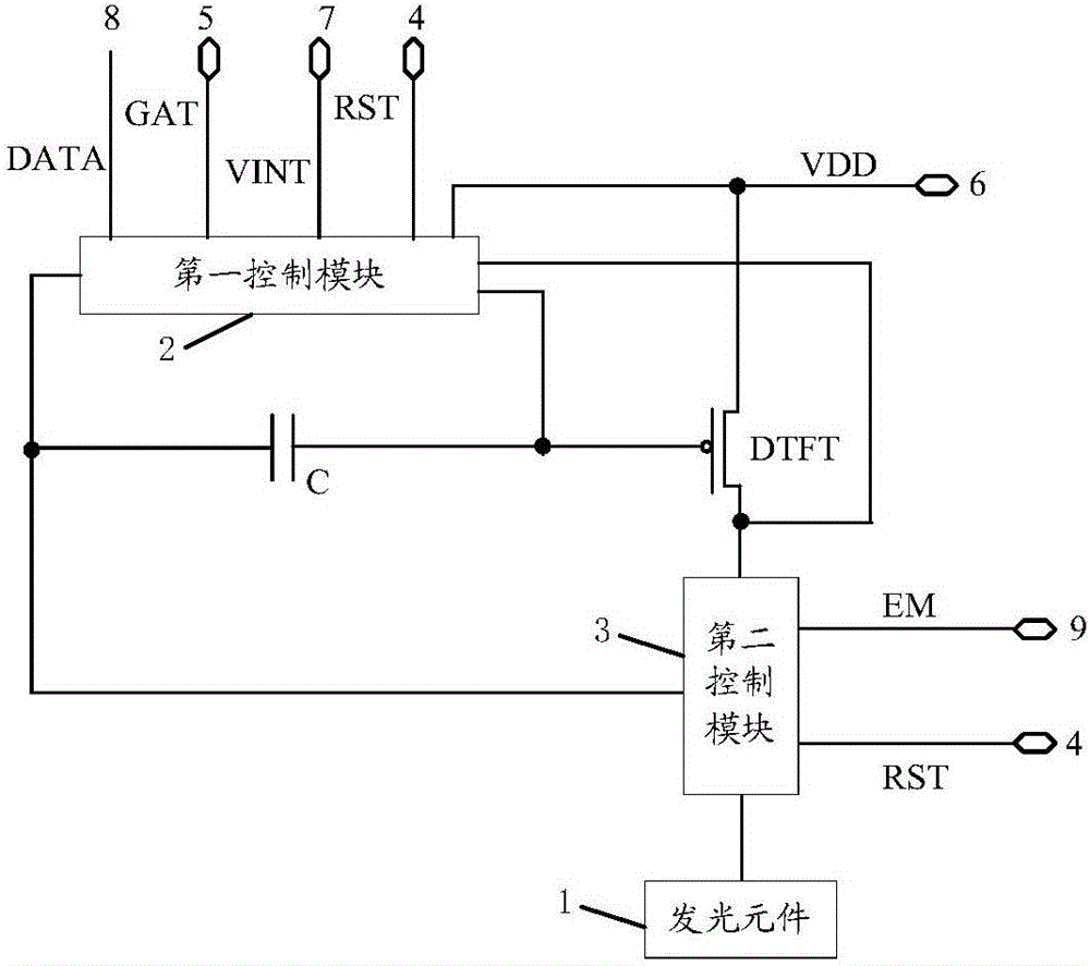
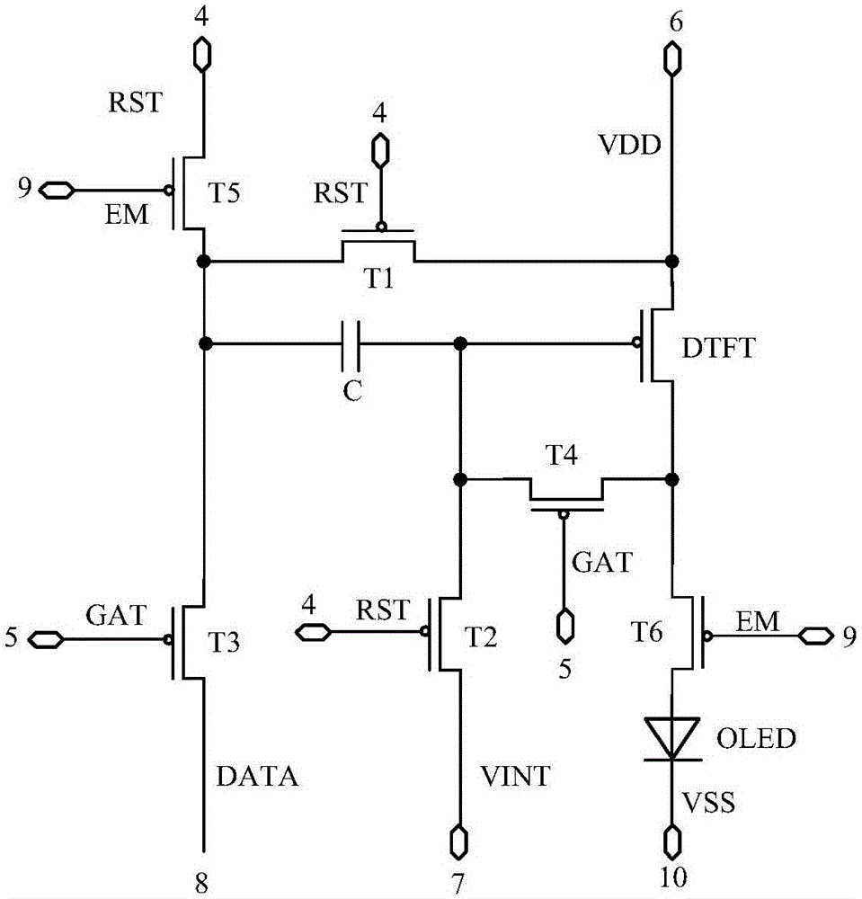
[0044] Such as figure 1 As shown, this embodiment provides a pixel driving circuit, the pixel driving circuit includes a driving transistor DTFT, a storage capacitor C and a light emitting element 1, in addition, the pixel driving circuit also includes a first control module 2 and a second control module 3 .

[0045]Wherein, the first control terminal of the first control module 2 is connected with the first pulse signal terminal 4, and the second control terminal of the first control module 2 is connected with the second pulse signal terminal 5; the first input terminal of the first control module 2 It is connected to the power supply signal terminal 6 and the source of the drive transistor DTFT, the second input terminal of the first control module 2 is connected to the initial signal terminal 7, the third input terminal of the first module is connected to the data line 8, and the second input terminal of the first module is connected to the data line 8. The four input term...

Embodiment 2

[0077] This embodiment provides a driving method for a pixel driving circuit, and the driving method for a pixel driving circuit is applied to the pixel driving circuit described in the first embodiment.

[0078] see again figure 1 The pixel driving circuit includes a driving transistor DTFT, a storage capacitor C, a light emitting element 1, a first control module 2 and a second control module 3, and the driving method of the pixel driving circuit specifically includes an initial period, a sampling period and a light emitting period.

[0079] Among them, in the initial period, the first pulse signal RST input by the first pulse signal terminal 4 controls the operation of the first control module 2, controls the transmission of the power supply signal VDD input by the power supply signal terminal 6 to the first plate of the storage capacitor C, and controls the initial signal The initial signal VINT input from the terminal 7 is transmitted to the second plate of the storage ca...

Embodiment 3

[0109] This embodiment provides a display device, and the display device includes the pixel driving circuit as described in the first embodiment.

[0110] Since the pixel driving circuit provided by Embodiment 1 reduces the number of signal lines for providing DC signals, the layout area occupied by the pixel driving circuit is reduced, and the corresponding number of pixels in the layout space is correspondingly increased. Therefore, compared with the prior art, the display device provided by this embodiment can achieve higher resolution, avoid the problem of poor Mura of vertical bars, and improve the brightness uniformity of the displayed picture.


PUM


Abstract

The invention provides a pixel driving circuit and a driving method thereof as well as a display device and belongs to the technical field of display. By means of the pixel driving circuit and the driving method thereof as well as the display device, the resolution of the display device can be increased, and the problem of poor vertical Mura is solved. The circuit comprises a driving transistor, a storage capacitor, a light emitting element, a first control module and a second control module, wherein a first control end and a second control end of the first control module are connected with a first impulse signal terminal and a second impulse signal terminal, a first input end is connected with a power supply signal terminal and a source of the driving transistor, a second input end is connected with an initial signal terminal, third and fourth input ends are connected with a data line and a drain of the driving transistor, a first output end is connected with a first pole plate of the storage capacitor, and a second output end is connected with a second pole plate and a grid of the driving transistor; a control end of the second control module is connected with a third impulse signal terminal, a first input end is connected with a first or second impulse signal terminal, a second input end is connected with the drain of the driving transistor, a first output end is connected with the first pole plate, and a second output end is connected with the light emitting element. The pixel driving circuit is used for increasing the resolution.

Description

technical field [0001] The present invention relates to the field of display technology, in particular to a pixel driving circuit, a driving method thereof, and a display device. Background technique [0002] In recent years, AMOLED (Active Matrix / Organic Light Emitting Diode, Active Matrix / Organic Light Emitting Diode) displays have been widely used due to their advantages such as fast response speed and high contrast ratio. Correspondingly, various pixel driving circuits for driving AMOLED display pixels to display have also been developed one after another. [0003] A traditional pixel driving circuit generally includes a driving transistor, a storage capacitor and a light emitting element. The storage capacitor provides a voltage stabilization signal for the gate of the driving transistor, thereby controlling the light emitting element to be in a stable light emitting state. In the prior art, a DC signal is usually used as a voltage-stabilizing signal, so an additional ...

Claims


Application Information

Patent Timeline
Patent Type & Authority Applications(China)
IPC IPC(8): G09G3/3266G09G3/3241
CPCG09G3/3241G09G3/3266G09G3/3233G09G2300/0819G09G2300/0842G09G2300/0861G09G2310/0251G09G2320/045G09G3/2096G09G3/3258G09G3/3291
Inventor 姚远高永益龙跃董婉俐
Owner BOE TECH GRP CO LTD
Why Eureka
Try Eureka