Forming method and array substrate of test pads

A technology for testing pads and array substrates, used in semiconductor/solid-state device testing/measurement, electrical components, electrical solid-state devices, etc. Effect

Active Publication Date: 2017-05-10
WUHAN CHINA STAR OPTOELECTRONICS TECH CO LTD
View PDF3 Cites 2 Cited by
  • Summary
  • Abstract
  • Description
  • Claims
  • Application Information

AI Technical Summary

Problems solved by technology

However, the traditional design is p...

Method used


Image

  • Forming method and array substrate of test pads
  • Forming method and array substrate of test pads
  • Forming method and array substrate of test pads

Examples


Embodiment 1

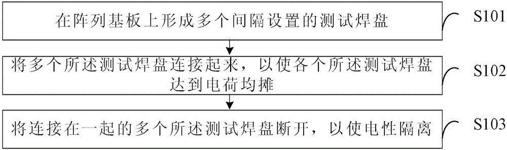
[0050] see figure 1 , is a schematic flowchart of the implementation of the method for forming the test pad provided by the embodiment of the present invention.

[0051] The method for forming the test pad includes:

[0052] In step S101, a plurality of test pads arranged at intervals are formed on the array substrate;

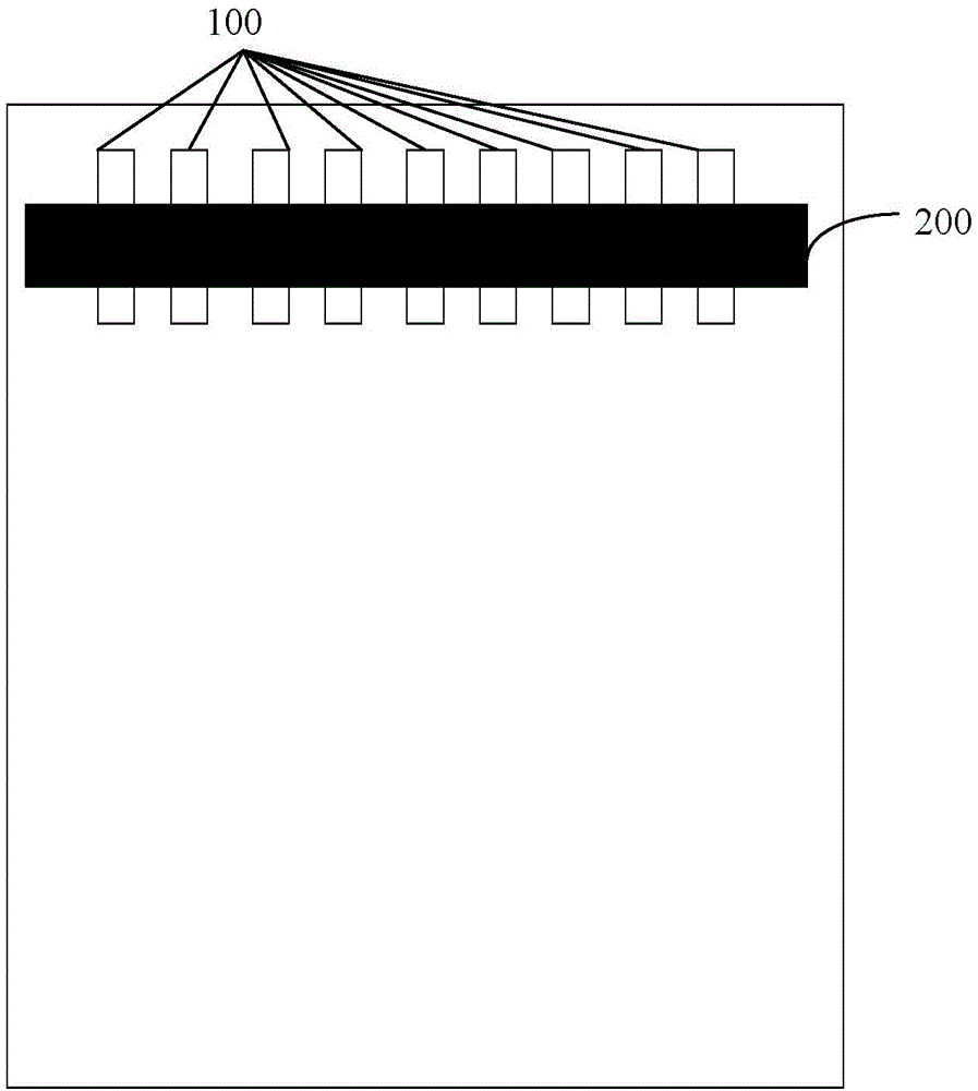
[0053] In some embodiments, for the display panel of the mobile phone, a plurality of test pads arranged at intervals are formed on the side of the array substrate. For example, a plurality of test pads arranged at intervals are formed on the upper and lower sides of the array substrate, such as image 3 shown.

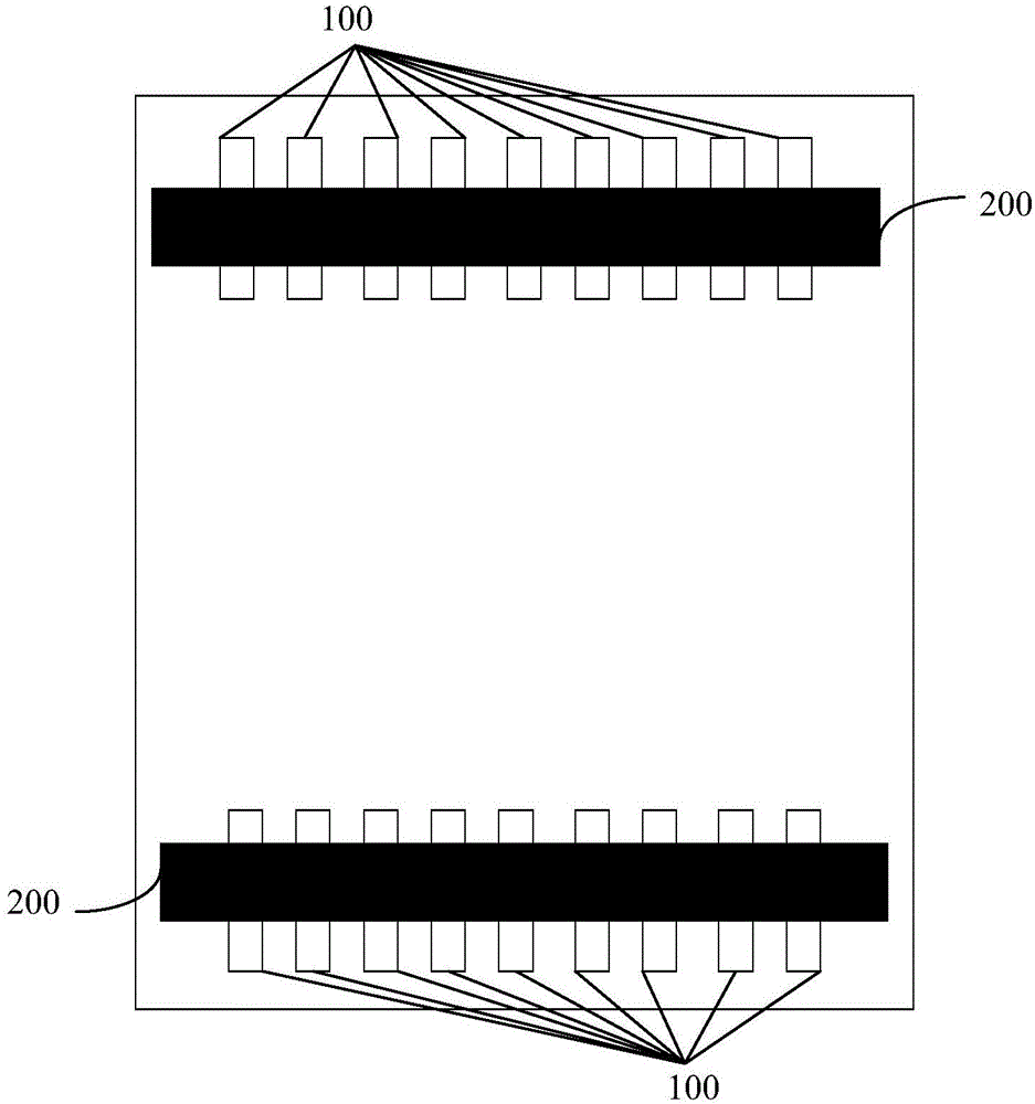
[0054] In some embodiments, for a liquid crystal display panel, a plurality of test pads arranged at intervals are formed around the array substrate, such as Figure 4 shown.

[0055] In step S102, connecting a plurality of the test pads, so that each of the test pads can achieve charge sharing;

[0056] In the embodiment of the present inventio...


PUM


Abstract

The invention discloses a forming method and an array substrate of test pads. The forming method includes that: a plurality of test pads arranged at intervals are formed on the array substrate; the test pads are connected to enable equal sharing of charge; the test pads are disconnected and electrically isolated. According to the forming method, in a manufacturing process, all the test pads are connected before different electrical signals are input into the test pads respectively, and then the test pads are disconnected before a test to enable accumulated charge to be equally distributed on the test pads before the test, so that an effect of risk sharing is achieved. The array substrate of the test pads is simple in structure and capable of preventing electro-static attacking.

Description

[0001] 【Technical field】 [0002] The invention relates to the technical field of display manufacturing, in particular to a method for forming a test pad and an array substrate. [0003] 【Background technique】 [0004] With the gradual popularization of LTPS (Low Temperature Poly-silicon, low-temperature polysilicon technology) panels, the array circuit design is becoming more and more refined. Small-sized panels PPI (Pixels Per Inch, which represents the number of pixels per inch) In addition, the risk of electrostatic damage is gradually increasing in the process of fine-fabricating array circuits, and ESD (Electro-Static discharge, electrostatic discharge) protection is becoming more and more important. [0005] In practice, the inventors found that the prior art has at least the following problems: [0006] After the TEST PAD (test pad) is formed, ESD occurs during the film formation and etching of the PV (Passivation Layer, passivation layer). The traditional protection ...

Claims


Application Information

Patent Timeline
IPC IPC(8): H01L21/66H01L27/12
CPCH01L22/32H01L27/1214
Inventor 李安石
Owner WUHAN CHINA STAR OPTOELECTRONICS TECH CO LTD
Why Eureka
Try Eureka