
Circuit board

A circuit board, transparent and conductive technology, applied in the direction of printed circuits, printed circuits, printed circuit components, etc., can solve the problems of less solder pads, large wiring area, affecting soldering quality, etc. The amount of paste and the effect of improving soldering yield

Inactive Publication Date: 2017-04-26
NANCHANG O FILM OPTICAL ELECTRONICS TECH CO LTD +3
View PDF9 Cites 1 Cited by
  • Summary
  • Abstract
  • Description
  • Claims
  • Application Information

AI Technical Summary

Problems solved by technology

In the prior art, the edge of the window (that is, the edge of the insulating layer) is outside the pad, that is, the window is larger than the pad, and there is a gap between the edge of the window and the edge of the pad. When the solder paste is coated on the pad or when the solder paste melts, the solder paste easily flows to the gap, resulting in too little tin on the pad, which affects the soldering quality; in the prior art, the size of the pad is often made larger than the actual need Larger size to cover the insulation to the edge of the pad, however, this takes up more routing area and is not suitable for boards with limited area and space

Method used


Image

  • Circuit board
  • Circuit board
  • Circuit board

Examples


Embodiment Construction

[0030] The technical solutions in the embodiments of the present invention will be clearly described below with reference to the drawings in the embodiments of the present invention.

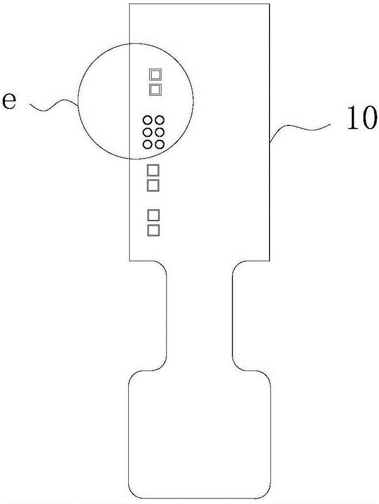
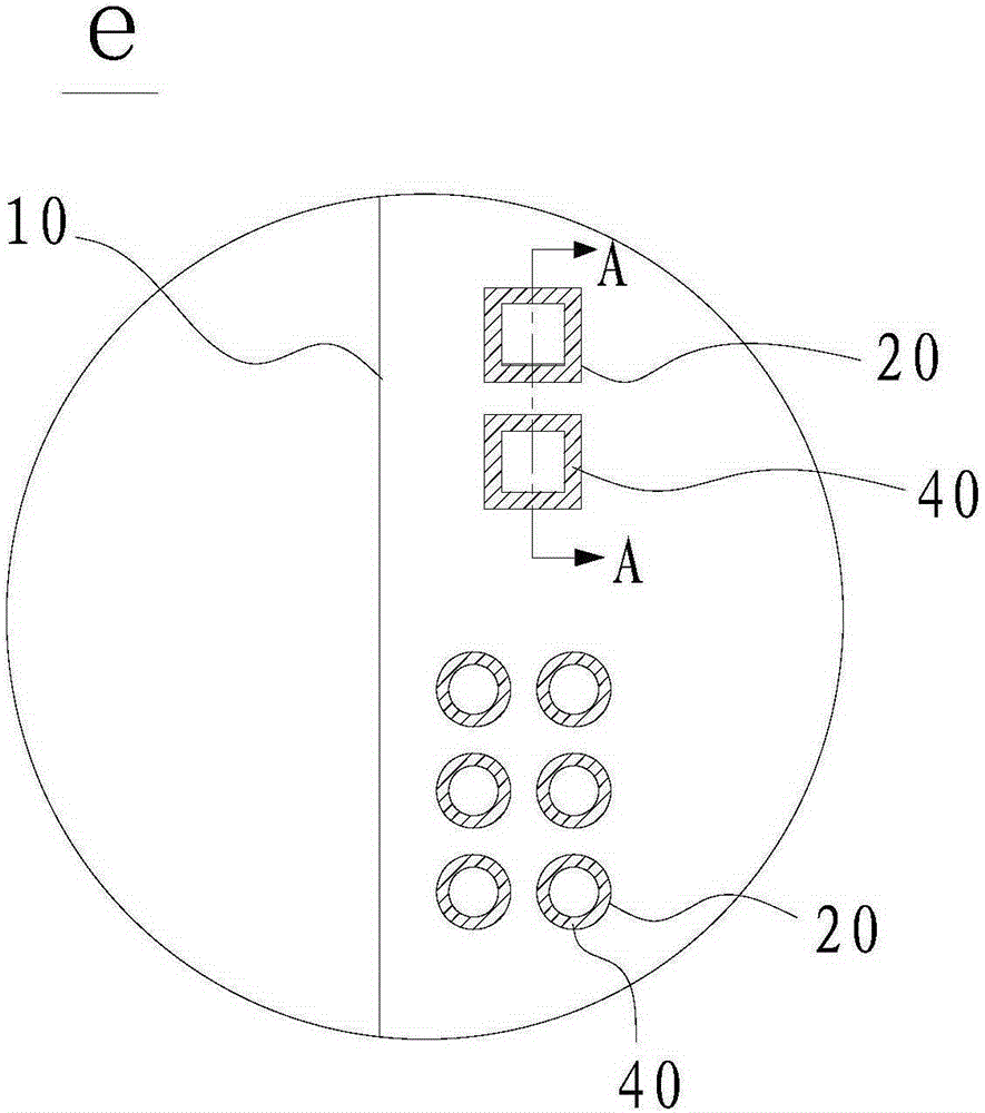
[0031] Please also see figure 1 , Figure 2a , Figure 2b and Figure 2c , The circuit board of the present invention includes a circuit board main body 10 , pads 20 , insulating layer 30 and transparent conductive adhesive layer 40 . The pad 20 and the insulating layer 30 are disposed on the main body 10 of the circuit board, and the insulating layer 30 is provided with a window 31 corresponding to the position of the pad 20 to expose the pad 20. The shape is consistent with the shape of the pad 20, and the pad 20 may be polygonal, circular or other geometric figures, and correspondingly, the window 31 is also polygonal, circular or other geometric figures. Preferably, the pad 20 is rectangular or circular. The number of the windows 31 is the same as the number of the pads 20 , that is, on...


PUM


Abstract

The invention discloses a circuit board comprising a main circuit board body, bonding pads, an insulating layer and transparent conductive adhesive layers. The bonding pads and the insulating layers are arranged on the main circuit board body; windows are formed at the positions, corresponding to the bonding pads, of the insulating layer to expose the bonding pads; and the edges, at the windows, of the insulating layer are close to the outer walls of the bonding pads. And the transparent conductive adhesive layers are arranged at one part of edges or all edges of the bonding pads. Therefore, exposure of wires connected with the bonding pads can be avoided; and the loss of the solder pastes on the bonding pads can be prevented.

Description

technical field [0001] The invention relates to the field of circuit boards, in particular to a circuit board with pads. Background technique [0002] In various electronic products, such as camera modules, mobile phones, electronic watches, etc., circuit boards are usually used to electrically connect various components of the electronic products or form various driving circuits. For example, the surface of the circuit board of the camera module is usually provided with components such as image sensors, capacitors and resistors, wherein the components such as capacitors and resistors are electrically connected to the circuit board through Surface Mounted Technology (SMT). Surface mount technology usually requires a pad on the circuit board. When mounting, first print solder paste on the pad, and then align the corresponding parts of the capacitor, resistor and other components with the pad to The components are accurately installed on the fixed position of the circuit boar...

Claims


Application Information

Patent Timeline
IPC IPC(8): H05K1/11
CPCH05K1/11H05K2201/09445
Inventor 刘燕妮雷光辉
Owner NANCHANG O FILM OPTICAL ELECTRONICS TECH CO LTD
Learn More