1*N demultiplexer/multiplexer optimization method
An optimization method and combiner technology, applied in design optimization/simulation, instruments, special data processing applications, etc., can solve problems such as high production process accuracy requirements and complex structure, and achieve the effect of avoiding poor optimization results
- Summary
- Abstract
- Description
- Claims
- Application Information
AI Technical Summary
Problems solved by technology
Method used
Image
Examples
Embodiment 1
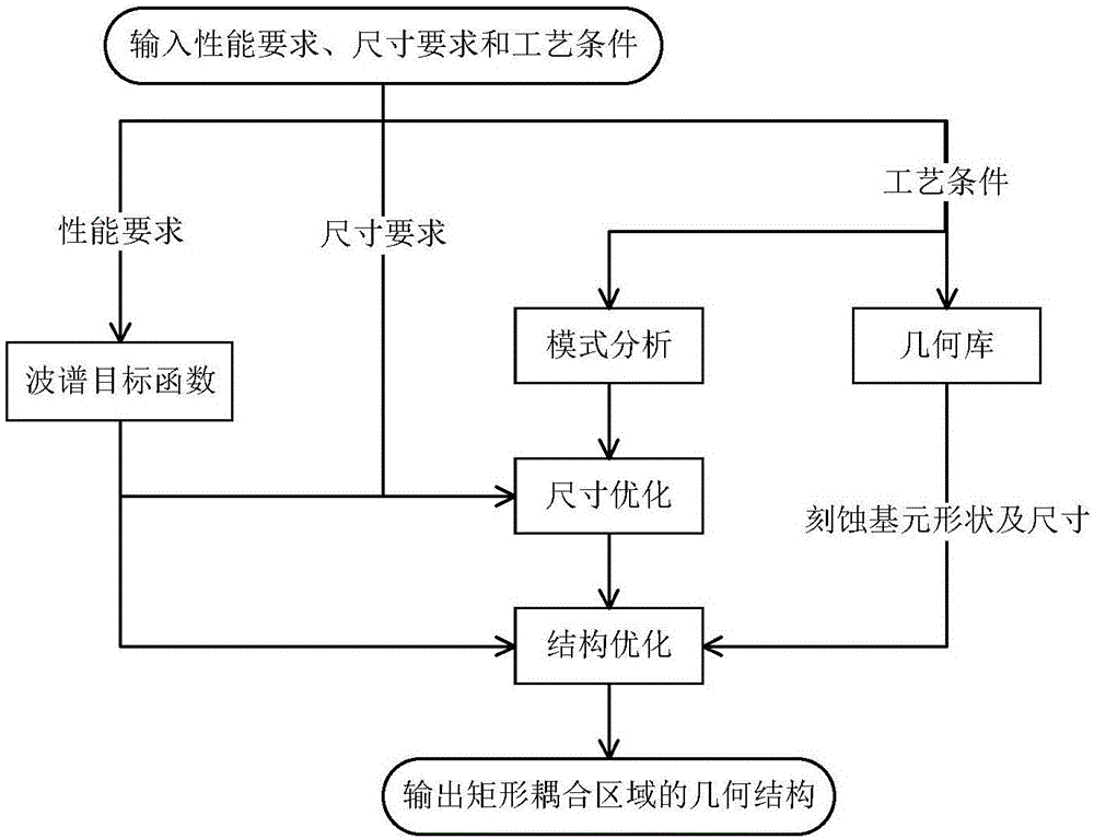
[0033] A method for optimizing a 1×N demultiplexer / combiner, which is applied to the optimization of a 1×21310nm / 1550nm demultiplexer / combiner, comprising the following steps:
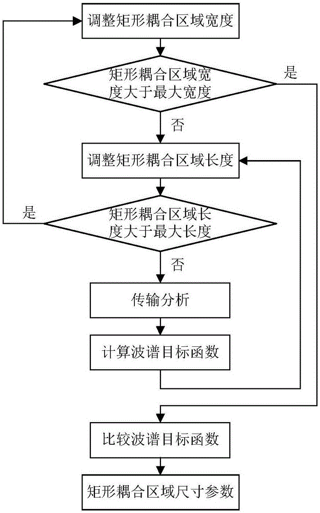
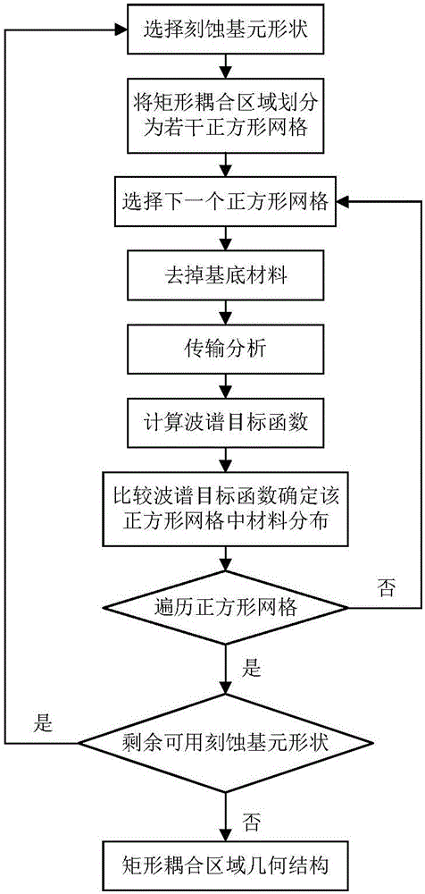
[0034] Step 1 Determine the performance requirements, size requirements and process conditions of the 1×21310nm / 1550nm wavelength demultiplexer, the performance requirements are at 1310nm and 1550nm wavelengths, when the power input to the input port is unit power, the output to the output port 1 target power a 11 and a 12 1 and 0, respectively, the target power output to output port 2 a 21 and a 22 are 0 and 1 respectively; the size requirement is the maximum size of the rectangular coupling area, where the maximum length L of the rectangular coupling area max 5000μm, maximum width W max is 50 μm; the process conditions include two parts, the first part is the refractive index of each part of the waveguide, where the substrate refractive index n s is 1.4444, the core refractive index n o is 1.46...
PUM
 Abstract
Description
Claims
Application Information
 - R&D
- Intellectual Property
- Life Sciences
- Materials
- Tech Scout
- Unparalleled Data Quality
- Higher Quality Content
- 60% Fewer Hallucinations
Browse by: Latest US Patents, China's latest patents, Technical Efficacy Thesaurus, Application Domain, Technology Topic, Popular Technical Reports.
© 2025 PatSnap. All rights reserved.Legal|Privacy policy|Modern Slavery Act Transparency Statement|Sitemap|About US| Contact US: help@patsnap.com


