A kind of preparation method of electron microscope sample of flat glass
A technology for flat glass and electron microscope samples, applied in the field of glass, can solve problems such as affecting production cost and efficiency, gas phase defects, defect corrosion damage, etc.
- Summary
- Abstract
- Description
- Claims
- Application Information
AI Technical Summary
Problems solved by technology
Method used
Image

Examples
preparation example Construction
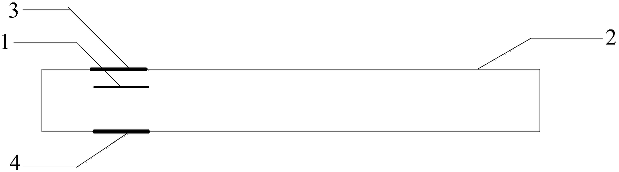
[0019] The invention provides a method for preparing an electron microscope sample of flat glass, wherein the flat glass 2 contains platinum crystallization 1, wherein the preparation method comprises:
[0020] S1. Determine the position of the platinum crystallization 1 in the flat glass 2, and mark the two surfaces of the flat glass 2 corresponding to the position as the first marking area 3 and the second marking area 4; determine where the first marking area 3 is located The distance between the surface of the first mark area 3 and the platinum crystallization 1; the distance between the surface of the first marking area 3 and the platinum crystallization 1 is not greater than the distance between the surface of the second marking area 4 and the platinum crystallization 1 ;
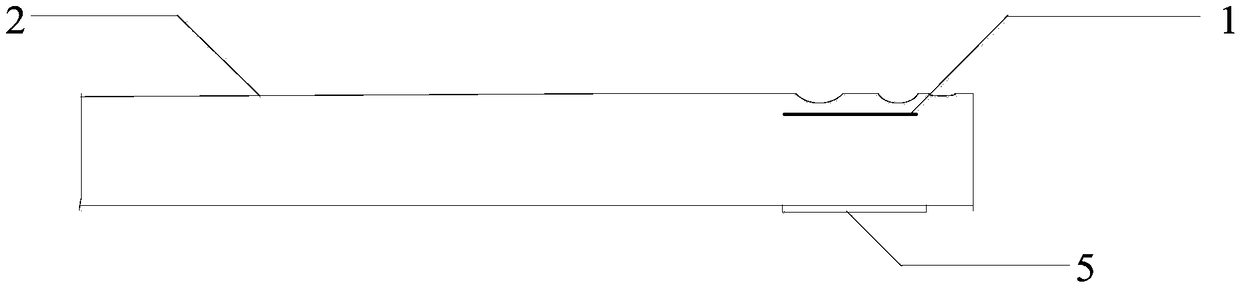
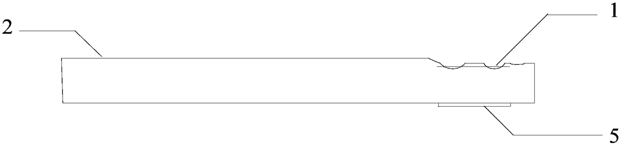
[0021] S2, grinding the first marking area 3, so that the first marking area 3 forms a rough surface, and covering the second marking area 4 with an anti-corrosion film 5;
[0022] S3. Etching the fi...
Embodiment 1
[0035] S1. Ultrasonic cleaning and drying the TFT-LCD substrate with platinum crystallization 1 defects inside, and confirming the position of platinum crystallization 1 in the TFT-LCD substrate through microscope observation, and the TFT-LCD substrate corresponding to the position The two surfaces of the two surfaces are respectively marked as the first marking area 3 and the second marking area 4 by drawing a circle with an oil-based marker pen; the distance between the surface where the first marking area 3 is located and the platinum crystallization 1 is determined by microscope observation; the first The distance between the surface where the marking area 3 is located and the platinum crystallization 1 is not greater than the distance between the surface where the second marking area 4 is located and the platinum crystallization 1; according to the first marking area relative to 1mm The distance corrosion time between the surface where 3 is located and the platinum crystal...
Embodiment 2
[0039]S1. Ultrasonic cleaning and drying the OLED device cover glass with platinum crystallization 1 defects inside, and confirming the position of platinum crystallization 1 in the OLED device cover glass through microscope observation, and the OLED device corresponding to the position The two surfaces of the cover glass are respectively marked as the first marking area 3 and the second marking area 4 by drawing lines with an oil-based marker; the distance between the surface where the first marking area 3 is located and the platinum crystallization 1 is determined by microscope observation The distance between the surface where the first marking area 3 is located and the platinum crystallization 1 is not greater than the distance between the surface where the second marking area 4 is located and the platinum crystallization 1; The distance corrosion time between the surface where the marking area 3 is located and the platinum crystallization 1 is 5h, and the time for the plat...
PUM
| Property | Measurement | Unit |
|---|---|---|
| length | aaaaa | aaaaa |
Abstract
Description
Claims
Application Information
 - Generate Ideas
- Intellectual Property
- Life Sciences
- Materials
- Tech Scout
- Unparalleled Data Quality
- Higher Quality Content
- 60% Fewer Hallucinations
Browse by: Latest US Patents, China's latest patents, Technical Efficacy Thesaurus, Application Domain, Technology Topic, Popular Technical Reports.
© 2025 PatSnap. All rights reserved.Legal|Privacy policy|Modern Slavery Act Transparency Statement|Sitemap|About US| Contact US: help@patsnap.com