Organic electroluminescence device substrate, display device and manufacturing method
A technology of organic light-emitting devices and electroluminescent devices, which is applied in the direction of organic semiconductor devices, semiconductor/solid-state device manufacturing, electric solid-state devices, etc., can solve the problems of discontinuous cathode film layer and poor cathode overlap, and achieve high transmission The effect of rate and display effect
- Summary
- Abstract
- Description
- Claims
- Application Information
AI Technical Summary
Problems solved by technology
Method used
Image
Examples
Embodiment 1
[0044] At least one embodiment of the present invention provides an organic electroluminescent device substrate, figure 2 It is a schematic structural view of the organic electroluminescent device substrate of at least one embodiment of the invention, such as figure 2 As shown, the organic electroluminescent device substrate of this embodiment may include a base substrate 1, a pixel defining layer 2 formed on the base substrate 1, and an organic light emitting diode formed in each pixel region defined by the pixel defining layer 2. device.
[0045] In this embodiment, the pixel defining layer 2 defines a plurality of pixel regions, which may be distributed in a matrix, and the plurality of pixel regions may be defined to emit light of the same or different colors. The pixel defining layer 2 has a top opening and a bottom opening corresponding to the opening area of each pixel area in the thickness direction perpendicular to the base substrate 1, and the bottom opening is ...
Embodiment 2
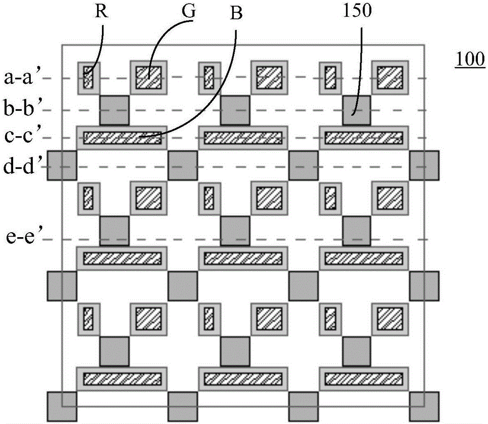
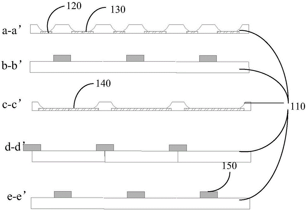
[0051] At least one embodiment of the present invention provides an organic electroluminescent device substrate 200, Figure 3A It is a schematic structural diagram of a pixel defining layer of an organic electroluminescent device substrate 200 according to at least one embodiment of the present invention, Figure 3B for Figure 3A The cross-sectional schematic diagrams of different parts of , where, Figure 3B The sections shown in a-a', b-b', c-c', d-d', e-e' are respectively along Figure 3A Pixels at the cutting lines a-a', b-b', c-c'd-d', e-e' of , define layer cross-sections.
[0052] Such as Figure 3A and 3B As shown, the organic electroluminescent device substrate 200 of this embodiment includes a base substrate, a pixel defining layer 210 formed on the base substrate 1, and an organic light emitting device formed in each pixel region defined by the pixel defining layer 210 , only the anode of the organic light emitting device is shown in the figure. The pixel d...
Embodiment 3
[0068] At least one embodiment of the present invention provides an organic electroluminescent display device, such as Image 6 As shown, the organic electroluminescent device substrate 300 described in any one of the embodiments is included. The organic electroluminescent display device in this embodiment may further include an opposite substrate 400, which is disposed on the organic electroluminescent device substrate 300, and the two are sealed together by a sealant, for example. The opposite substrate 400 may include a glass substrate. In practical applications, the organic electroluminescence display device can be realized as a mobile phone, a television, a computer, an instrument panel, and the like.
[0069] Since the organic electroluminescent display device of this embodiment has the organic electroluminescent device substrate of the above-mentioned embodiment, its technical effect is the same, so details will not be repeated here.
PUM
 Abstract
Description
Claims
Application Information
 - R&D Engineer
- R&D Manager
- IP Professional
- Industry Leading Data Capabilities
- Powerful AI technology
- Patent DNA Extraction
Browse by: Latest US Patents, China's latest patents, Technical Efficacy Thesaurus, Application Domain, Technology Topic, Popular Technical Reports.
© 2024 PatSnap. All rights reserved.Legal|Privacy policy|Modern Slavery Act Transparency Statement|Sitemap|About US| Contact US: help@patsnap.com


