A vertical structure root-enhanced field-effect transistor and its manufacturing method

A field-effect transistor and vertical structure technology, which is applied in the vertical structure GaN-based enhancement field-effect transistor and its manufacturing field, can solve the problems of device surface breakdown reduction, few research reports, breakdown voltage increase, etc., to increase output current , Improving the withstand voltage capability and facilitating packaging

Inactive Publication Date: 2020-05-12
HUNAN INSTITUTE OF SCIENCE AND TECHNOLOGY
View PDF6 Cites 0 Cited by
  • Summary
  • Abstract
  • Description
  • Claims
  • Application Information

AI Technical Summary

Problems solved by technology

[0007] When the vertical conductive structure is adopted, the probability of surface breakdown of the device is greatly reduced, and the breakdown voltage will be greatly improved, but there are few related research reports

Method used


Image

  • A vertical structure root-enhanced field-effect transistor and its manufacturing method
  • A vertical structure root-enhanced field-effect transistor and its manufacturing method
  • A vertical structure root-enhanced field-effect transistor and its manufacturing method

Examples


Embodiment 1

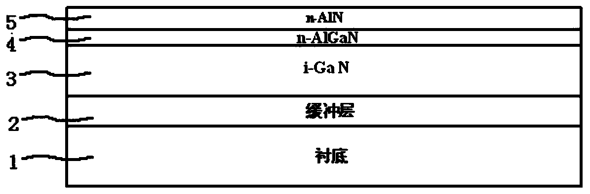
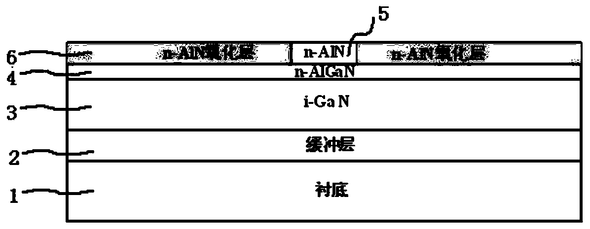
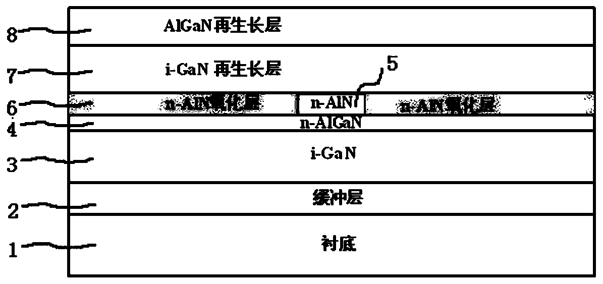
[0031] FIG. 1( h ) is a schematic diagram of the device structure of Example 1. Its structure includes substrate layer (1), buffer layer (2), unintentionally doped GaN (i-GaN) epitaxial layer (3), n-type AlGaN (n-AlGaN) epitaxial layer (4), n-type AlN (n -AlN) conductive layer (5) and n-AlN oxide layer (6), i-GaN regrowth layer (7), AlGaN regrowth layer (8), gate oxide layer (9), arranged on (8) The source (10), the drain (11) arranged on (4), and the gate (12) arranged on (9).

[0032] The manufacturing process flow of the above-mentioned vertical structure GaN-based enhancement mode field effect transistor is as follows:

[0033] A) As shown in Figure 1(a), a buffer layer (2), an i-GaN epitaxial layer (3), and an n-AlGaN layer are sequentially grown on a substrate (1) by metal-organic chemical vapor deposition (MOCVD) (4), n-AlN layer (5), the epitaxial growth temperature is between 1050°C and 1100°C, the substrate (1) is one of sapphire, silicon, silicon carbide or galliu...

Embodiment 2

[0042] like figure 2 It is a schematic diagram of the device structure of Example 2. It is similar to the device structure of Example 1, the only difference is that in step C of the manufacturing process flow, a secondary epitaxial growth containing i-GaN layer (7) and no + - Homojunction formed by GaN layers.


PUM


Abstract

The invention discloses a vertical-structure GaN-based enhancement mode field effect transistor and a manufacturing method therefor. The device comprises a substrate layer (1), a buffer layer (2), a non-intentionally-doped GaN (i-GaN) epitaxial layer (3), an n type AlGaN epitaxial layer (4), an n type AlN conductive layer (5), an n type AlN oxide isolation layer (6), an i-GaN regrowth layer (7), an AlGaN regrowth layer (8), a gate electrode oxide layer (9), a source electrode (10) arranged on the (8), a drain electrode (11) arranged on the (4), and a gate electrode (12) arranged on the (9). When the device is in use, the drain electrode current, by passing through the non-oxidized n type AlN conductive layer, flows to the source electrode to form the vertically and conductively structured enhancement mode device. The enhancement mode field effect transistor has the advantages of high breakdown voltage, high output current density, low leakage current and the like, and is suitable for the application in the field of the high-power electric power and electronics.

Description

technical field [0001] The invention relates to the field of semiconductor devices, in particular to a GaN-based enhancement field-effect transistor with a vertical structure and a manufacturing method thereof. Background technique [0002] As a representative of the third-generation wide-bandgap semiconductor materials, GaN materials have a wider bandgap (E g ) large, electron saturation drift velocity (v sat ) high, mobility (μ) high, thermal conductivity (k) large, critical electric field (E c ), low dielectric constant (ε), etc., so it is very suitable for making power electronic devices with high temperature resistance, high voltage resistance, high power, low loss, and high density integration. [0003] For power field effect transistors, it is generally required that the threshold voltage of the device is greater than 3V, that is, it is an enhanced device to ensure the "failure safety" of the circuit. In addition, the use of enhanced devices can effectively simplif...

Claims


Application Information

Patent Timeline
Patent Type & Authority Patents(China)
IPC IPC(8): H01L21/336H01L21/28H01L29/06H01L29/417H01L29/423
CPCH01L21/28H01L29/0607H01L29/0611H01L29/41741H01L29/4232H01L29/66477
Inventor 文于华刘阳
Owner HUNAN INSTITUTE OF SCIENCE AND TECHNOLOGY
Why Eureka
Try Eureka