GOA (Gate Driver On Array) circuit of liquid crystal display panel and display device
A liquid crystal display panel and circuit technology, applied in static indicators, instruments, etc., can solve the problems of lower potential of the second circuit point, easy leakage of thin film transistors, insufficient thrust of scanning signals, etc. Improve the effect of driving force
- Summary
- Abstract
- Description
- Claims
- Application Information
AI Technical Summary
Problems solved by technology
Method used
Image
Examples
Embodiment 1
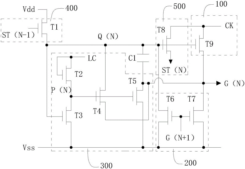
[0039] Please refer to figure 1 , figure 1 It is a schematic diagram of the overall structure of a COA circuit of a liquid crystal display panel in this embodiment, from figure 1 It can be seen that a COA circuit of a liquid crystal display panel of the present invention is used to drive cascaded scan lines, and includes a plurality of cascaded GOA units, wherein the Nth level GOA unit controls the Nth level scan line Charging is controlled, and the Nth-level GOA unit includes:
[0040] A pull-down sustaining circuit unit 300, configured to maintain low the scan signal corresponding to the scan line;
[0041] a pull-down circuit unit 200, configured to pull down the scan signal corresponding to the scan line;
[0042] a pull-up circuit unit 100, configured to pull up the corresponding scan signal of the scan line;
[0043] A pull-up and sustain circuit unit 400, configured to maintain and pull up the scan signal of the corresponding scan line;
[0044] The downlink circui...
Embodiment 2
[0070] A display device in this embodiment includes a liquid crystal display panel, and the liquid crystal display panel includes the COA circuit described in Embodiment 1. Since the COA circuit has been described in detail in Embodiment 1, it will not be repeated here. Discuss it.
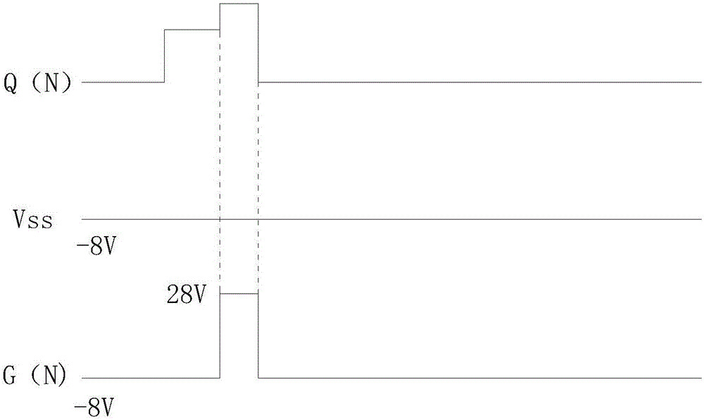
[0071] In a display device of the present invention, the COA circuit of its liquid crystal display panel connects the source and the drain of a thin film transistor of the pull-down sustaining circuit unit 300 to the second circuit point Q(N) and the scan line of the current stage respectively, thereby reducing the The potential difference between the source and the drain of the thin film transistor at the second circuit point Q(N) is reduced, so that the thin film transistor is not prone to electric leakage, and at the same time, the driving force of the scanning signal is improved to ensure the continuous transmission of the device.
PUM
 Abstract
Description
Claims
Application Information
 - R&D
- Intellectual Property
- Life Sciences
- Materials
- Tech Scout
- Unparalleled Data Quality
- Higher Quality Content
- 60% Fewer Hallucinations
Browse by: Latest US Patents, China's latest patents, Technical Efficacy Thesaurus, Application Domain, Technology Topic, Popular Technical Reports.
© 2025 PatSnap. All rights reserved.Legal|Privacy policy|Modern Slavery Act Transparency Statement|Sitemap|About US| Contact US: help@patsnap.com


