Primary control LED driving circuit based on SEPIC and Fly-back circuits
A technology of LED driving and primary side control, applied in electric light sources, electrical components, electroluminescent light sources, etc., can solve the problems of low power density, reduced working life and control accuracy of the system, and low reliability of the LED driver system. , to reduce the switching loss
- Summary
- Abstract
- Description
- Claims
- Application Information
AI Technical Summary
Problems solved by technology
Method used
Image
Examples
specific Embodiment approach 1
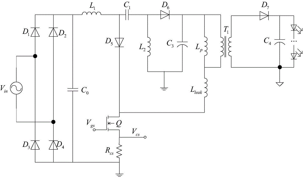
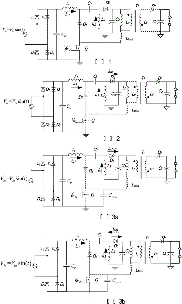
[0040] Embodiment 1: In the primary side control LED drive circuit based on SEPIC and Flyback circuit described in this embodiment, the 220V AC mains input circuit is electrically connected to the SEPIC circuit, the SEPIC circuit is electrically connected to the Flyback converter circuit, and the Flyback converter circuit Connect with the LED electrical appliances to be driven,
[0041] The SEPIC circuit is used for the power factor correction of the front stage,
[0042] The Flyback converter circuit is used to realize primary side control.
[0043] SEPIC circuit (single ended primary inductor converter, DC-DC converter that allows the output voltage to be greater than, less than or equal to the input voltage), in the circuit design stage, limits the input current ripple, so the low voltage at the input end of the circuit can be omitted. pass filter circuit. At the same time, the SEPIC circuit has the characteristics of step-up and step-down, which can be more flexible for ...
specific Embodiment approach 2
[0045] Specific implementation mode two: refer to figure 1 Describe this embodiment in detail. This embodiment is a further description of the primary side control LED drive circuit based on SEPIC and Flyback circuits described in the first specific embodiment. In this embodiment, the primary side control LED drive circuit includes: a diode D. 1 , Diode D 2, Diode D 3 , Diode D 4 , capacitance C 0 , inductance L 1 , Diode D 5 , capacitance C 1 , inductance L 2 , Diode D 6 , Bus capacitance C 3 , inductance L p , Transformer T 1 , Diode D 7 , inductance L leak , output capacitance C 4 , switch tube Q and resistor R cs ;
[0046] Diode D 1 The cathode of the diode D 2 negative pole, capacitor C 0 one end and the inductance L 1 connected at one end,
[0047] Diode D 3 Anode, diode D 4 positive electrode and capacitor C 0 The other end is connected to the power ground at the same time,
[0048] Diode D 1 the anode of the diode D 3 connected to the catho...
PUM
 Abstract
Description
Claims
Application Information
 - R&D
- Intellectual Property
- Life Sciences
- Materials
- Tech Scout
- Unparalleled Data Quality
- Higher Quality Content
- 60% Fewer Hallucinations
Browse by: Latest US Patents, China's latest patents, Technical Efficacy Thesaurus, Application Domain, Technology Topic, Popular Technical Reports.
© 2025 PatSnap. All rights reserved.Legal|Privacy policy|Modern Slavery Act Transparency Statement|Sitemap|About US| Contact US: help@patsnap.com


