Touch substrate, preparation method thereof and touch display device

A technology for touch display devices and substrates, which is applied in the fields of optics, instruments, and electrical digital data processing, etc., and can solve problems such as reduced product competitiveness, loss of touch functions of touch devices, and rising production costs, so as to improve competitiveness, The effect of reducing production costs and preventing breakdown and conduction

Active Publication Date: 2017-01-25
BOE TECH GRP CO LTD +1
View PDF9 Cites 23 Cited by
  • Summary
  • Abstract
  • Description
  • Claims
  • Application Information

AI Technical Summary

Problems solved by technology

During the production or use of the touch device, electrostatic accumulation often occurs in the area where the light-shielding pattern 50 is in contact with the dummy electrode 30. When the static electricity accumulation reaches a certain level, the light-shielding pattern 50 will be broken down, thereby making the light-shielding pattern 50 conductive. As shown in FIG. 1( b ), a conductive channel is formed in the region of the gap 40, and the conductive channel formed by the dummy electrode 30 and the gap 40 connects the first touch electrodes 10 in different columns or the second touch electrodes 20 in different rows. Together they form a micro-short circuit, which eventually leads to the loss of the touch function of the touch device
[0005] In the prior art, major touch device manufacturers improve the anti-ESD (Electro-Static discharge, electrostatic discharge) capability of the light-shielding area 01 of the touch device mainly by combining the light-shielding pattern 50 with the first touch screen during the production process. An insulating layer (such as SiO2, etc.) is added between the electrode 10, the second touch electrode 20 and the dummy electrode 30 to avoid the micro-short circuit caused by the breakdown of the light-shielding pattern 50. Although this can effectively reduce the occurrence probability of ESD, the While increasing the insulation layer, the production cost will increase, which will eventually lead to a decrease in product competitiveness

Method used


Image

  • Touch substrate, preparation method thereof and touch display device
  • Touch substrate, preparation method thereof and touch display device
  • Touch substrate, preparation method thereof and touch display device

Examples


Embodiment Construction

[0032] The following will clearly and completely describe the technical solutions in the embodiments of the present invention with reference to the accompanying drawings in the embodiments of the present invention. Obviously, the described embodiments are only some, not all, embodiments of the present invention. Based on the embodiments of the present invention, all other embodiments obtained by persons of ordinary skill in the art without making creative efforts belong to the protection scope of the present invention.

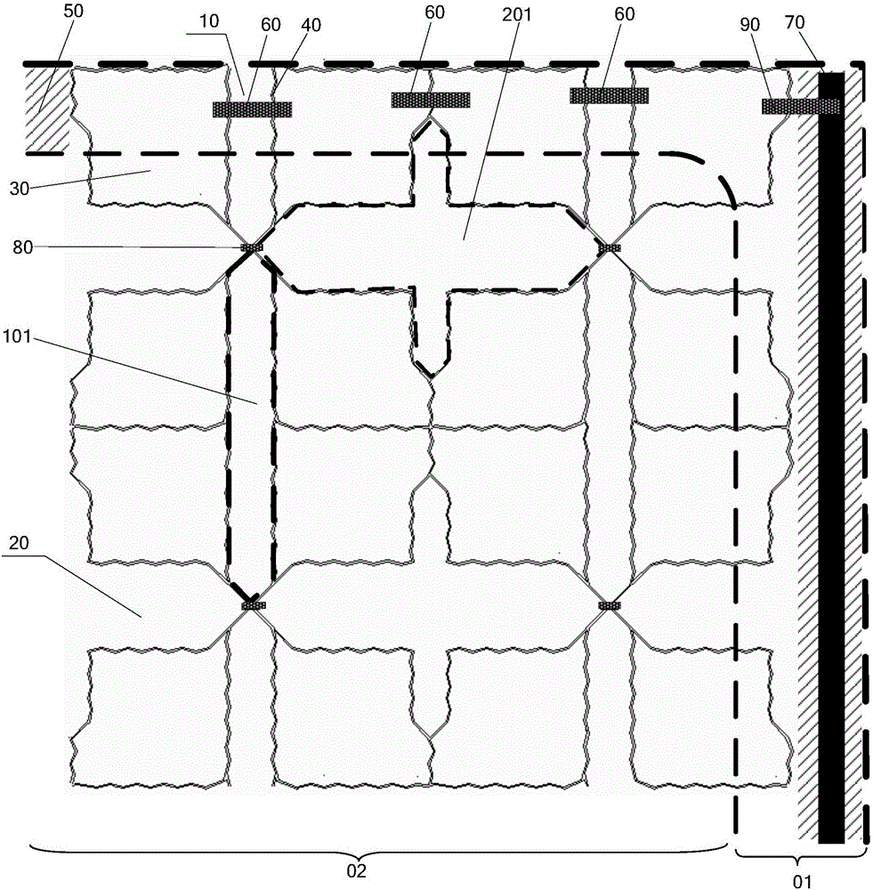
[0033] An embodiment of the present invention provides a touch substrate, such as figure 2As shown, it is divided into a touch area 02 and a light-shielding area 01 surrounding the touch area. A light-shielding pattern 50 is arranged in the light-shielding area 01. The touch substrate includes a first touch electrode 10 and a second touch electrode that cross and are insulated from each other. 20, and a dummy electrode 30 arranged in the area defined by the fi...


PUM


Abstract

The embodiment of the invention provides a touch substrate, a preparation method thereof and a touch display device, and relates to the technical field of display. Static on virtual electrodes in a shading zone can be released, and compared with the prior art, production cost can be reduced. The touch substrate is divided into a touch zone and the shading zone encircling the touch zone, and a shading pattern is arranged in the shading zone. The touch substrate comprises first touch electrodes, second touch electrodes and the virtual electrodes, wherein the first touch electrodes and the second touch electrodes intersect and are insulated from each other, the virtual electrodes are arranged in a zone defined by the first touch electrodes and the second touch electrodes, and gaps exit between the virtual electrodes and the first touch electrodes and between the virtual electrodes and the second touch electrodes. The first touch electrodes, the second touch electrodes and the virtual electrodes make contact with the shading pattern, the parts, located in the shading zone, of the adjacent virtual electrodes are connected through first bridges, and the first bridges are insulated from the first touch electrodes and the second touch electrodes. A first ground wire is arranged in the shading zone and electrically connected with the virtual electrodes connected through the first bridges.

Description

technical field [0001] The present invention relates to the field of display technology, in particular to a touch substrate, a preparation method thereof, and a touch display device. Background technique [0002] Since the rise of touch technology, due to its simplicity, speed, and humanization, the popularity of touch technology has become higher and higher, and there are more and more products with touch functions on the market, including mobile phones, tablets and notebook computers. Wait. [0003] At present, as shown in FIG. 1(a), the touch device includes a first touch electrode 10 and a second touch electrode 20. Taking FIG. 1(a) as an example, the first touch electrode 10 includes a plurality of directly connected The first sub-touch electrodes 101 and the second touch electrodes 20 include a plurality of second sub-touch electrodes 201 disconnected from each other. Adjacent second sub-touch electrodes 201 are connected by bridges, and the bridges are connected to t...

Claims


Application Information

Patent Timeline
Patent Type & Authority Applications(China)
IPC IPC(8): G06F3/041
CPCG06F3/0412G06F2203/04103G06F3/0445G06F3/0446G02F1/13338G02F1/1343G06F3/041
Inventor 王静张明谢晓冬何敏李冬
Owner BOE TECH GRP CO LTD
Why Eureka
Try Eureka