Method for self-assembly of nanomaterials to form a substrate with a ring pattern and the formed substrate with a ring pattern and applications
A technology of nanomaterials and ring patterns, which is applied in the field of self-assembly of nanomaterials to form substrates with ring patterns, which can solve the problems of high cost and complicated process
- Summary
- Abstract
- Description
- Claims
- Application Information
AI Technical Summary
Problems solved by technology
Method used
Image
Examples
Embodiment 1
[0053] This embodiment is used to illustrate the substrate with a ring pattern and its assembly method of the present invention.
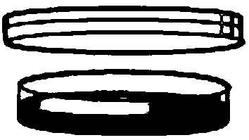
[0054] use figure 1 device, wherein the base material is polystyrene, and polystyrene is also used to form an annular outer wall around the base material, thus forming such as figure 1 The circular dish shown (35mm in diameter) was cleaned ultrasonically with deionized water, followed by ethanol and blown dry with nitrogen.
[0055] Multi-walled carbon nanotubes (purchased from Shenzhen Nanotech Port Co., Ltd, L-MWNT-1020 grade, 10-20 nm in diameter, about 2-5 μm in length) and SDBS (the mass ratio of multi-walled carbon nanotubes and SDBS is 0.1 : 1) adding into water and ultrasonically dispersing for 4 hours to obtain a dispersion A1 with a carbon nanotube concentration of 0.3 mg / mL.
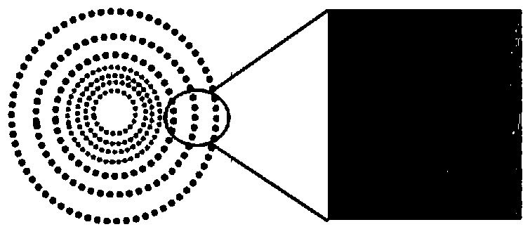
[0056] Add the dispersion A1 to the above-mentioned circular vessel, so that the distance between the bottom surface of the formed meniscus and the base material...
Embodiment 2
[0058] This embodiment is used to illustrate the substrate with a ring pattern and its assembly method of the present invention.
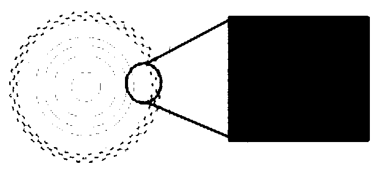
[0059] According to the method described in Example 1, the difference is that the base material is polystyrene after the surface is gold-plated, and the annular pattern formed on the base is as follows: image 3 As shown, the ring distribution of the ring pattern formed on the substrate is: from the center to the edge, followed by smooth circular line distribution, wavy line distribution, and a certain connection distribution between the rings, and the single ring width is 10-30 μm. The ring spacing is 10-100 μm.
Embodiment 3
[0061] This embodiment is used to illustrate the substrate with a ring pattern and its assembly method of the present invention.
[0062] According to the method described in embodiment 1, the difference is that the base material is glass, and the annular pattern formed on the base is as Figure 4 As shown, the single ring is a smooth circular line distribution, the single ring width is 5-40 μm, and the ring spacing is 50-200 μm.
PUM
| Property | Measurement | Unit |
|---|---|---|
| size | aaaaa | aaaaa |
| size | aaaaa | aaaaa |
| size | aaaaa | aaaaa |
Abstract
Description
Claims
Application Information
 - R&D
- Intellectual Property
- Life Sciences
- Materials
- Tech Scout
- Unparalleled Data Quality
- Higher Quality Content
- 60% Fewer Hallucinations
Browse by: Latest US Patents, China's latest patents, Technical Efficacy Thesaurus, Application Domain, Technology Topic, Popular Technical Reports.
© 2025 PatSnap. All rights reserved.Legal|Privacy policy|Modern Slavery Act Transparency Statement|Sitemap|About US| Contact US: help@patsnap.com


