
A chip anti-electromagnetic interference high-frequency inductance element

An anti-electromagnetic interference, inductive element technology, applied in the direction of preventing/reducing unwanted electrical/magnetic effects, etc., can solve the problems of the adverse effect of the inductive element's operation, the inductive element not working normally, and the large contact area between the top and the outside world. , to achieve the effect of stable installation, strong anti-electromagnetic interference ability and simple structure

Active Publication Date: 2018-01-19
合肥博雷电气有限公司
View PDF6 Cites 0 Cited by
  • Summary
  • Abstract
  • Description
  • Claims
  • Application Information

AI Technical Summary

Problems solved by technology

[0002] The harm of electromagnetic interference to the public environment and personal safety has been recognized by countries all over the world. Shielding technology, one of the three major technologies for suppressing electromagnetic interference, shielding, grounding and filtering, is currently the most effective and economical means of suppressing electromagnetic interference. The method used is very Simple, installing a shielding device on the electrical components can greatly reduce the electromagnetic interference to the electrical components, so that the electrical components can work normally. The top of the existing inductive component has a large contact area with the outside world, so it is easily affected by external electromagnetic interference. The operation of the inductance element is adversely affected, so that the inductance element cannot work normally

Method used


Image

  • A chip anti-electromagnetic interference high-frequency inductance element

Examples


Embodiment Construction

[0012] The following will clearly and completely describe the technical solutions in the embodiments of the present invention with reference to the accompanying drawings in the embodiments of the present invention. Obviously, the described embodiments are only some, not all, embodiments of the present invention.

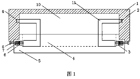
[0013] refer to figure 1 , a chip-type anti-electromagnetic interference high-frequency inductance element, including an inductance body 5 and a shielding device 1, the top of the inductance body 5 is provided with a first groove 4, and two Us are slidably connected to the inner wall of the bottom of the first groove 4 type column 11, and two U-shaped columns 11 are arranged opposite to each other, one end of the U-shaped column 11 is provided with a clamping column 2, and the inner walls of both sides of the first groove 4 are provided with a first fixed circular hole, and the first fixed circular hole The inner wall of the hole is connected with a fixed cylinder 3,...


PUM


Abstract

The invention discloses a chip type anti-electromagnetic interference high-frequency inductance element which comprises an inductance body and a shielding device, wherein a first groove is formed at the top of the inductance body; the bottom inner wall of the first groove is glidingly connected with two U-shaped columns which are oppositely arranged; a clamp column is arranged at one end of the U-shaped column; a first fixing round hole is formed on the two side inner walls of the first groove respectively; the inner wall of the first fixing round hole is connected with a fixing cylinder; a second fixing round hole is formed at the two ends of the fixing cylinder respectively; the inner wall of the second fixing round hole is glidingly connected with a fixing rod; a push plate is arranged at the end of the fixing rod away from the first groove and positioned on the outer side of the inductance body; and the other end of the fixing rod is connected with the other end of the U-shaped column. The chip type anti-electromagnetic interference high-frequency inductance element disclosed by the invention has simple structure and high stability and is economical and practical and facilitates the mounting of a shielding device; and moreover, due to the strong anti-electromagnetic interference ability of the high-frequency inductance element, the inductance element can run normally.

Description

technical field [0001] The invention relates to the technical field of anti-electromagnetic interference high-frequency inductive elements, in particular to a chip-type anti-electromagnetic interference high-frequency inductive element. Background technique [0002] The harm of electromagnetic interference to the public environment and personal safety has been recognized by countries all over the world. Shielding technology, one of the three major technologies for suppressing electromagnetic interference, shielding, grounding and filtering, is currently the most effective and economical means of suppressing electromagnetic interference. The method used is very Simple, installing a shielding device on the electrical components can greatly reduce the electromagnetic interference to the electrical components, so that the electrical components can work normally. The top of the existing inductive component has a large contact area with the outside world, so it is easily affected b...

Claims


Application Information

Patent Timeline
Patent Type & Authority Patents(China)
IPC IPC(8): H01F27/36
CPCH01F27/36
Inventor 刘英高龙芮庆
Owner 合肥博雷电气有限公司
Learn More