A multi-mode soft-switching lossless absorber
A non-destructive absorption and soft switching technology, which is applied in the direction of output power conversion device, climate sustainability, high-efficiency power electronic conversion, etc., can solve the inconsistency of switching energy absorption effect, the deterioration of switching energy absorption effect, and the output of component parameters Voltage instability and other problems, to achieve the effect of improving power utilization efficiency, reducing environmental electromagnetic interference, and improving service life
- Summary
- Abstract
- Description
- Claims
- Application Information
AI Technical Summary
Problems solved by technology
Method used
Image
Examples
Embodiment 1
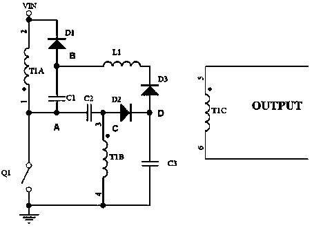
[0022] A multi-mode soft-switching lossless absorber, such as figure 1 As shown, it includes primary winding T1A, auxiliary winding T1B and secondary winding T1C of the single-ended converter, switching tube Q1, capacitors C1, C2, C3, diodes D1, D2 and inductor L1, wherein: T1A and T1C form a single-ended positive Exciting or single-ended flyback converter, T1B is an auxiliary winding with the same number of turns as T1A, the function is to make the voltage across C2 equal to VIN, C3, D3, L1, C1, Q1 form a resonant circuit, composed of Q1, C2, D2, C3 constitutes the switch tube clamp absorption circuit, and Q1, C1, D1 form another switch tube clamp absorption circuit.
[0023] The connection relationship of each component is: point A connects single-ended transformer primary winding T1A, switch tube Q1, capacitor C1 and capacitor C2, point B connects the anode of diode D1, capacitor C1 and inductor L1, and point C connects capacitor C2 and diode D2 Positive pole and unilatera...
Embodiment 2
[0036] Another embodiment of the multi-mode soft-switching lossless absorption device is, as figure 2 As shown, one end of the capacitor C3 is connected to the cathode of the diode D2, and the other end is connected to the power supply terminal VIN. In this connection mode, the voltage conditions on H, I, J, and K are the same as those on A, B, C, and D above, except that the voltage at both ends of C3 changes accordingly due to different reference points.
[0037] In a word, the present invention has following effect:
[0038] 1. When the switch tube Q1 is turned on and off, it is clamped by the capacitor and diode circuit connected to it, which strongly suppresses the peak voltage, thereby achieving a smooth switching close to zero voltage, and reducing the environmental electromagnetic caused by the switch tube being turned on and off. interference.
[0039] 2. Reduce the voltage and current that the switching tube bears when it is turned on and off, and improve the serv...
PUM
 Abstract
Description
Claims
Application Information
 - R&D
- Intellectual Property
- Life Sciences
- Materials
- Tech Scout
- Unparalleled Data Quality
- Higher Quality Content
- 60% Fewer Hallucinations
Browse by: Latest US Patents, China's latest patents, Technical Efficacy Thesaurus, Application Domain, Technology Topic, Popular Technical Reports.
© 2025 PatSnap. All rights reserved.Legal|Privacy policy|Modern Slavery Act Transparency Statement|Sitemap|About US| Contact US: help@patsnap.com


