Wireless charging system suitable for low-power-consumption wireless sensor network node equipment
A wireless sensor and network node technology, applied in network topology, wireless communication, electrical components, etc., can solve the problem of inability to meet the needs of charging, and achieve the effects of high energy receiving efficiency, convenient use, and reduced damage
- Summary
- Abstract
- Description
- Claims
- Application Information
AI Technical Summary
Problems solved by technology
Method used
Image
Examples
Embodiment 1
[0029] Embodiment 1 Overall working principle of the present invention
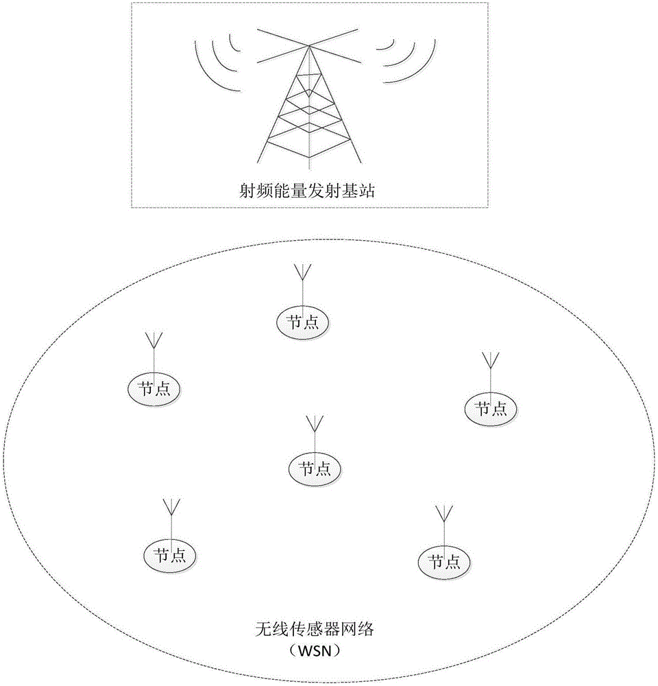
[0030] refer to figure 1 The structure of the wireless charging system suitable for low-power wireless sensor network node equipment based on wireless radio frequency energy harvesting technology of the present invention is composed of a radio frequency energy transmitting base station and a wireless sensor network node. The radio frequency energy transmitting base station transmits radio frequency energy to the direction of the node through the directional transmitting antenna, and the receiving antenna on the low-power wireless sensor network node within the coverage of the radio frequency energy transmitting base station receives the radio frequency energy for charging the load battery.
Embodiment 2
[0031] Embodiment 2 General framework of the present invention
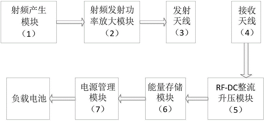
[0032] refer to figure 2, the structure of the wireless charging system suitable for low-power wireless sensor network node equipment based on wireless radio frequency energy harvesting technology of the present invention is: radio frequency generation module 1, radio frequency transmission power amplification module 2, transmission antenna 3, reception antenna 4, RF -DC rectification and boosting module 5 , energy storage module 6 and power management module 7 . Wherein the radio frequency generation module 1 is responsible for generating the required 500MHz radio frequency signal; the radio frequency transmission power amplification module 2 is responsible for amplifying the power of the radio frequency signal generated by the radio frequency generation module 1 to be transmitted; the transmitting antenna 3 is responsible for passing through the radio frequency transmission power amplification module 2. The r...
Embodiment 3
[0033] Embodiment 3 The radio frequency generation module 1 of the present invention
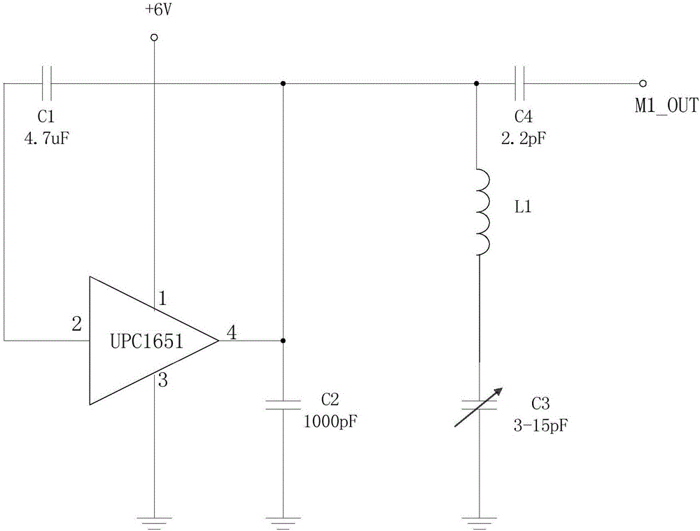
[0034] refer to image 3 , the structure of the radio frequency generation module 1 is: the pin 1 of the chip UPC1651 is connected to the +6v power supply, the pin 3 is grounded, the pin 4 is grounded through the capacitor C2, the capacitor C1 is connected between the pin 4 and the pin 2, and the lead Pin 4 is also connected to one end of the capacitor C4 and one end of the inductor L1, the other end of the inductor L1 is connected to one end of the variable capacitor C3, the other end of the variable capacitor C3 is grounded, and the other end of the capacitor C4 is used as the output end of the radio frequency generation module 1, Denoted as port M1_OUT. Adjust the variable capacitor so that the output frequency is 500MHz, and this module provides 500MHz radio frequency for the entire transmitter.
PUM
 Abstract
Description
Claims
Application Information
 - Generate Ideas
- Intellectual Property
- Life Sciences
- Materials
- Tech Scout
- Unparalleled Data Quality
- Higher Quality Content
- 60% Fewer Hallucinations
Browse by: Latest US Patents, China's latest patents, Technical Efficacy Thesaurus, Application Domain, Technology Topic, Popular Technical Reports.
© 2025 PatSnap. All rights reserved.Legal|Privacy policy|Modern Slavery Act Transparency Statement|Sitemap|About US| Contact US: help@patsnap.com


