Quantum dot light-emitting device, backlight module and liquid crystal display device
A technology of quantum dot light-emitting and light-emitting device, which is applied in optics, nonlinear optics, instruments, etc., can solve the problems of reducing the light extraction efficiency and light energy loss of the quantum dot layer, improve the conversion efficiency of absorption excitation light, and reduce the secondary conversion. , the effect of reducing conversions
- Summary
- Abstract
- Description
- Claims
- Application Information
AI Technical Summary
Problems solved by technology
Method used
Image
Examples
Embodiment 1
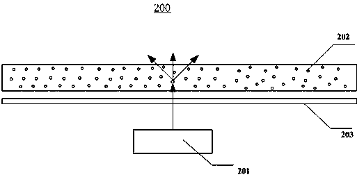
[0037] figure 2 A schematic structural diagram of a quantum dot light-emitting device is provided for Embodiment 1 of the present invention, as shown in figure 2 As shown, the quantum dot light-emitting device 300 includes: a light-emitting device 301, a second quantum dot encapsulation layer 302 and a third quantum dot encapsulation layer 303, the light-emitting device 301 generates excitation light with a first wavelength, and the second quantum dot encapsulation layer 302 uses The third quantum dot encapsulation layer 303 is used to absorb the excitation light of the first wavelength to generate the second wavelength conversion light by absorbing the excitation light of the first wavelength, and the second quantum dot encapsulation layer 302 is located in the light emitting device 301 Between the third quantum dot encapsulation layer 303, wherein the third wavelength is smaller than the second wavelength and larger than the first wavelength.
[0038]Exemplarily, the ligh...
Embodiment 2
[0048] Figure 4 A schematic structural diagram of a package is provided for the quantum dot light-emitting device in the first embodiment of the second embodiment of the present invention, as shown in image 3 As shown, a quantum dot light-emitting device package 50 can be used as a light source for a backlight in a backlight module, and can be used alone as a lighting source, including:
[0049] The circuit board 51 is arranged to provide a power circuit for the quantum dot light emitting device package 50 .
[0050] The light emitting device 52 is arranged on the circuit board 51 and generates excitation light with a first wavelength. Wherein, the light emitting device 52 may be a light emitting diode (LED) chip, such as a GaN-based LED chip that emits blue light.
[0051] The second quantum dot encapsulation layer 53 is used for absorbing the exciting light of the first wavelength to generate the second wavelength converted light.
[0052] The third quantum dot encapsul...
Embodiment 3
[0062] Figure 5 A schematic structural diagram of a quantum dot light-emitting device package is provided in Embodiment 3 of the present invention, as shown in Figure 5 As shown, a quantum dot light-emitting device package 60 can be used as a light source, used as a backlight source in a backlight module, and can be used alone as a lighting source.
[0063] Quantum dot light emitting device package 60 includes:
[0064] The packaging base 62 is formed in a groove shape.
[0065] The light emitting device 61 is arranged on the bottom of the groove of the packaging substrate 62 to generate excitation light of the first wavelength. Wherein, the light emitting device 61 may be a light emitting diode (LED) chip, such as a GaN-based LED chip that emits blue light.
[0066] The second quantum dot encapsulation layer 63 is used for absorbing the excitation light of the first wavelength to generate the second wavelength conversion light.
[0067] The third quantum dot encapsulati...
PUM
| Property | Measurement | Unit |
|---|---|---|
| diameter | aaaaa | aaaaa |
Abstract
Description
Claims
Application Information
 - Generate Ideas
- Intellectual Property
- Life Sciences
- Materials
- Tech Scout
- Unparalleled Data Quality
- Higher Quality Content
- 60% Fewer Hallucinations
Browse by: Latest US Patents, China's latest patents, Technical Efficacy Thesaurus, Application Domain, Technology Topic, Popular Technical Reports.
© 2025 PatSnap. All rights reserved.Legal|Privacy policy|Modern Slavery Act Transparency Statement|Sitemap|About US| Contact US: help@patsnap.com


