A light-emitting diode epitaxial structure with adjustable warpage during growth

A technology of light-emitting diodes and epitaxial structures, applied in electrical components, circuits, semiconductor devices, etc., can solve problems such as temperature changes, abnormal epitaxial surfaces, abnormal electrical properties, etc. The effect of performance and product yield

Active Publication Date: 2018-06-01
XIAMEN CHANGELIGHT CO LTD
View PDF7 Cites 0 Cited by
  • Summary
  • Abstract
  • Description
  • Claims
  • Application Information

AI Technical Summary

Problems solved by technology

[0006] The purpose of the present invention is to provide a light-emitting diode epitaxial structure with adjustable warpage during the growth process, so as to solve the problem of epitaxial wafer bending caused by temperature changes and internal stress problems when growing epitaxial layers with different functions during the epitaxial growth process of the substrate, and Epitaxial surface abnormalities and electrical performance abnormalities caused by increased bending of epitaxial wafers

Method used


Image

  • A light-emitting diode epitaxial structure with adjustable warpage during growth
  • A light-emitting diode epitaxial structure with adjustable warpage during growth
  • A light-emitting diode epitaxial structure with adjustable warpage during growth

Examples


Embodiment Construction

[0040] The present invention will be described in detail below in conjunction with the accompanying drawings and specific embodiments.

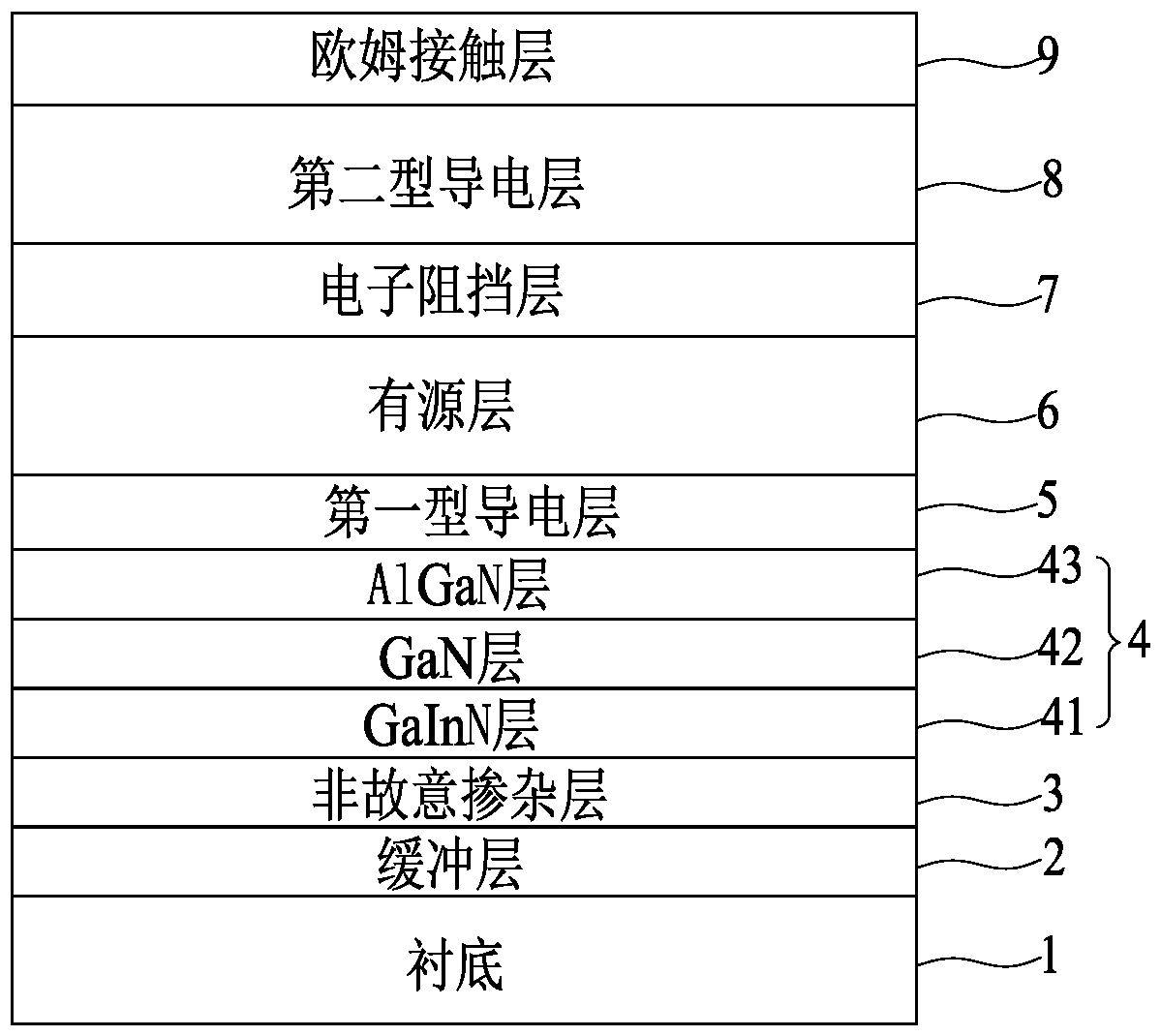
[0041] refer to image 3 As shown, the present invention discloses a light-emitting diode epitaxial structure with adjustable warpage during the growth process. A buffer layer 2 is grown on the substrate 1, an unintentionally doped layer 3 is grown on the buffer layer 2, and an unintentionally doped layer 3 is grown on the unintentionally doped layer 3. Growth composite adjustment layer 4, first-type conductive layer 5 is grown on composite adjustment layer 4, active layer 6 is grown on first-type conductive layer 5, electron blocking layer 7 is grown on active layer 6, and second-type conductive layer is grown on electron blocking layer 7 The second-type conductive layer 8 , on which the ohmic contact layer 9 grows. The substrate 1 is preferably a large-scale sapphire substrate.

[0042] The composite adjustment layer 4 is one of GaInN / GaN...


PUM


Abstract

The invention discloses a light-emitting diode epitaxial structure with an adjustable warping growth process. A buffer layer, an unintentionally doped layer, a composite adjustment layer, a first type conductive layer, an active layer, an electron blocking layer, a second type conductive layer and an ohmic contact layer sequentially grow on a substrate from bottom to top; and the composite adjustment layer is one of GaInN / GaN / AlGaN and AlGaN / GaN / GaInN. By the light-emitting diode epitaxial structure, the problems of epitaxial wafer bending caused by a temperature change or an internal stress problem when epitaxial layers with different functions grow in the epitaxial growth process, and an abnormal epitaxial surface and the abnormal electrical property caused by an epitaxial wafer bending increase are solved.

Description

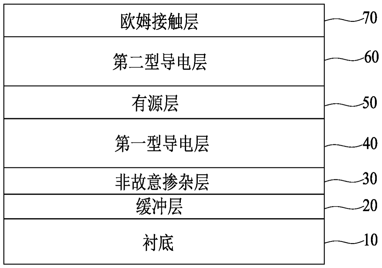
technical field [0001] The invention relates to the technical field of light-emitting diodes, in particular to an epitaxial structure of light-emitting diodes with adjustable warpage during growth. Background technique [0002] like figure 1 As shown, in the conventional light-emitting diode epitaxial structure disclosed in the prior art, a buffer layer 20 is vapor-deposited on the substrate 10 by PVD, and the buffer layer 20 is an AlN buffer layer, or a GaN buffer layer, or an AlGaN buffer layer; growing an unintentionally doped layer (uGaN) 30 on the buffer layer 20; growing a first-type conductive layer (nGaN) 40 on the unintentionally doped layer 30; growing an active layer ( MQW) 50 ; a second-type conductive layer (pGaN) 60 is grown on the active layer (MQW) 50 ; an ohmic contact layer (ITO) 70 is grown on the second-type conductive layer (pGaN) 60 . [0003] like Figure 2a As shown, when growing the unintentionally doped layer (uGaN) on the buffer layer, if the wa...

Claims


Application Information

Patent Timeline
Patent Type & Authority Patents(China)
IPC IPC(8): H01L33/04H01L33/12H01L33/14H01L33/00
CPCH01L33/0066H01L33/04H01L33/12H01L33/145
Inventor 林志伟陈凯轩张永卓祥景姜伟汪洋童吉楚方天足
Owner XIAMEN CHANGELIGHT CO LTD
Why Eureka
Try Eureka