


Quick Research
Generate reliable direction feasibility study reports for your R&D in just a few steps.

Technical Q&A
Discover and master advanced knowledge NOW. Basics, ideas, possibilities, all at once.

Find Solutions
As an expert in R&D theories, this can generate solutions to your technical problems instantly.

Evaluate Feasibility
Analyze your overall solution with one click, know your potential R&D risks in advance.

Monitor Landscape
Get weekly tech updates, stay abreast of the latest tech innovations and key insights.
Method for adjusting warping degree of wafer, and semiconductor device
A warpage and wafer technology, applied in semiconductor/solid-state device manufacturing, electrical components, circuits, etc., can solve problems such as reducing the performance and yield of semiconductor devices, the impact of back-end processes, and wafer warpage deformation.
- Summary
- Abstract
- Description
- Claims
- Application Information
AI Technical Summary
Problems solved by technology
Method used
Image

Examples
Embodiment approach
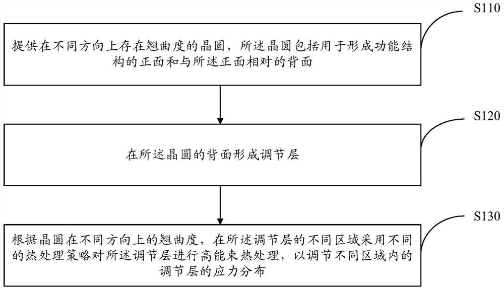
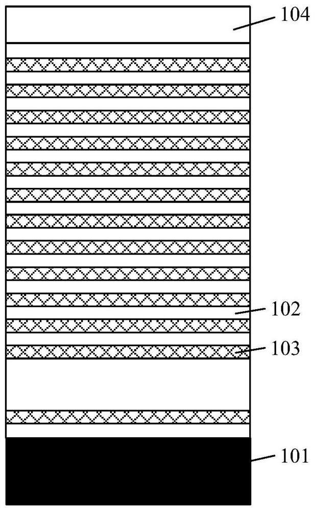
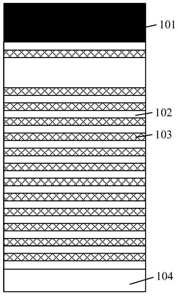
[0068] In one embodiment, according to the warpage of the wafer in different directions, high-energy beam heat treatment is performed on each region in the adjustment layer, wherein at least some regions adopt different heat treatment parameters than other regions except this part of the region. The heat treatment parameters of the wafer can be used to make this part of the region and other regions generate different stresses, thereby selectively reducing the warpage of different regions of the wafer. The heat treatment parameters include heat treatment temperature and heat treatment time. Therefore, it may be that the heat treatment time adopted by at least a part of the region is different from the heat treatment time of other regions except this part of the region; or, the heat treatment temperature adopted by at least a part of the region is different from the heat treatment temperature of other regions except this part of the region; or , the temperature and time of heat ...
PUM
 Abstract
Description
Claims
Application Information
 - R&D Engineer
- R&D Manager
- IP Professional
- Industry Leading Data Capabilities
- Powerful AI technology
- Patent DNA Extraction
Browse by: Latest US Patents, China's latest patents, Technical Efficacy Thesaurus, Application Domain, Technology Topic, Popular Technical Reports.
© 2024 PatSnap. All rights reserved.Legal|Privacy policy|Modern Slavery Act Transparency Statement|Sitemap|About US| Contact US: help@patsnap.com