Transparent conductive film
A technology of transparent conductive film and transparent conductive layer, which is applied in the direction of synthetic resin layered products, coatings, chemical instruments and methods, etc., can solve the problems of poor appearance and easy identification of electrostatic capacitive touch panels, and achieve inhibition Effect of dissolving or falling off, inhibiting adhesion
- Summary
- Abstract
- Description
- Claims
- Application Information
AI Technical Summary
Problems solved by technology
Method used
Image
Examples
no. 1 Embodiment approach
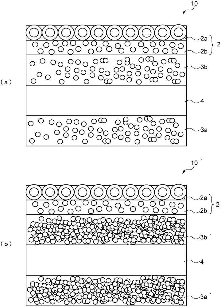
[0053] The first embodiment of the present invention is a laminate 10 for forming a transparent conductive layer, such as figure 1 As shown in (a), it is a laminate 10 for forming a transparent conductive layer formed by sequentially laminating a hard coat layer 3a, a base film 4, and an optical adjustment layer 2, and is characterized in that the hard coat layer 3a is It is obtained by photocuring a composition for forming a hard coat layer containing the following components (A) to (B):
[0054] (A) active energy ray curable resin 100 parts by weight,
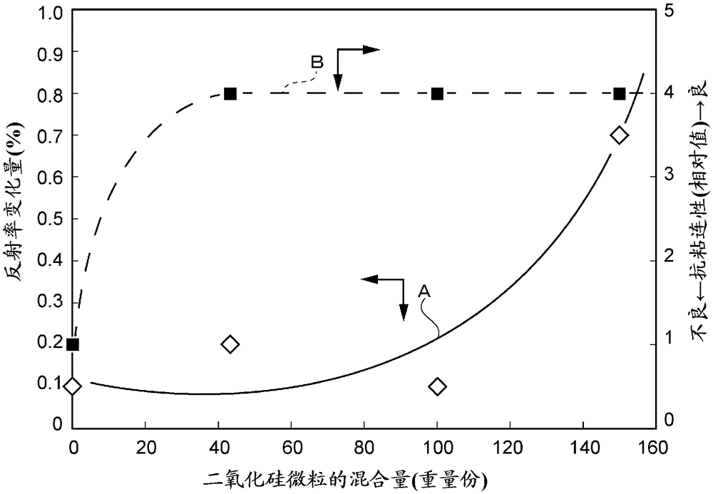
[0055] (B) Silica fine particles 15 to 100 parts by weight.
[0056] It should be noted that in figure 1 In (a), the laminate 10 for forming a transparent conductive layer having a hard coat layer 3 (3a, 3b) on both surfaces of the base film 4 is shown as an example, but the base film 4 and the optical adjustment layer The hard coating 3b between 2 can be omitted.
[0057] In addition, the optical adjustment layer 2 is sh...
no. 2 Embodiment approach
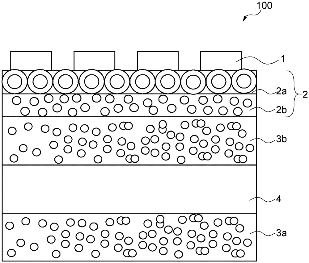
[0261] The second embodiment of the present invention is a transparent conductive film, such as image 3 As shown, it is a transparent conductive film formed by sequentially laminating a hard coat layer, a base film, an optical adjustment layer and a transparent conductive layer. It is characterized in that the hard coat layer will contain the following (A)~ The composition for forming a hard coat layer of the component (B) is photocured:
[0262] (A) active energy ray curable resin 100 parts by weight,
[0263] (B) Silica particles 15 to 100 parts by weight.
[0264] Hereinafter, the second embodiment of the present invention will omit parts that overlap with the previous content, and only the different parts will be described in detail.
[0265] 1. Transparent conductive layer
[0266] (1) Raw material
[0267] In the transparent conductive film of the present invention, the raw material of the transparent conductive layer is not particularly limited as long as it has bo...
Embodiment 1
[0294] 1. Preparation of Hard Coat Forming Composition
[0295] Active energy ray curable resin as component (A), silica fine particles as component (B), leveling agent as component (C) and photopolymerization initiator as component (D) are housed in the container with the following composition After the preparation, a solvent was added and mixed uniformly to prepare a composition for forming a hard coat layer having a solid content concentration of 22% by weight.
[0296] It should be noted that the following compositions and the mixing amounts of the compositions shown in Table 1 represent pure components from which the diluting solvent has been removed.
[0297] (A) Component: dipentaerythritol hexaacrylate 100 parts by weight
[0298] (B) Component: Reactive solid silica particles 43.2 parts by weight
[0299] (Volume average particle diameter (D50) 15nm)
[0300] (C) Component: Fluorine leveling agent 0.05 parts by weight
[0301] (Neos Co., Ltd., Ftergent 7602A)
[...
PUM
| Property | Measurement | Unit |
|---|---|---|
| thickness | aaaaa | aaaaa |
| thickness | aaaaa | aaaaa |
| thickness | aaaaa | aaaaa |
Abstract
Description
Claims
Application Information
 - R&D
- Intellectual Property
- Life Sciences
- Materials
- Tech Scout
- Unparalleled Data Quality
- Higher Quality Content
- 60% Fewer Hallucinations
Browse by: Latest US Patents, China's latest patents, Technical Efficacy Thesaurus, Application Domain, Technology Topic, Popular Technical Reports.
© 2025 PatSnap. All rights reserved.Legal|Privacy policy|Modern Slavery Act Transparency Statement|Sitemap|About US| Contact US: help@patsnap.com


