Camera element and camera device
A technology for imaging elements and imaging conditions, which is applied in the field of electronic equipment, imaging devices and imaging elements, and can solve problems such as difficulty in application, difficulty in generating images, and insufficient convenience in the use of electronic equipment, so as to achieve a reasonable exposure effect
- Summary
- Abstract
- Description
- Claims
- Application Information
AI Technical Summary
Problems solved by technology
Method used
Image

Examples
no. 1 approach -
[0071] Hereinafter, a first embodiment of the present invention will be described with reference to the drawings. However, the present invention is not limited thereto. In addition, in the drawings, in order to describe the embodiment, a part may be enlarged or emphasized, and the scale may be changed appropriately. In addition, in each of the following embodiments, an interchangeable-lens digital camera will be described as an example of an electronic device.
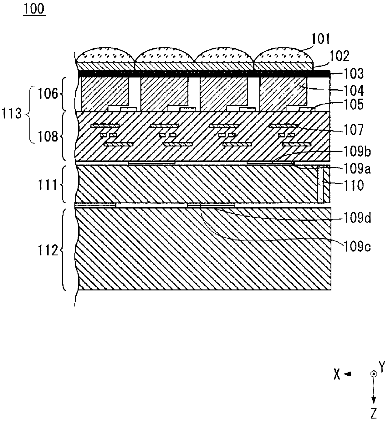
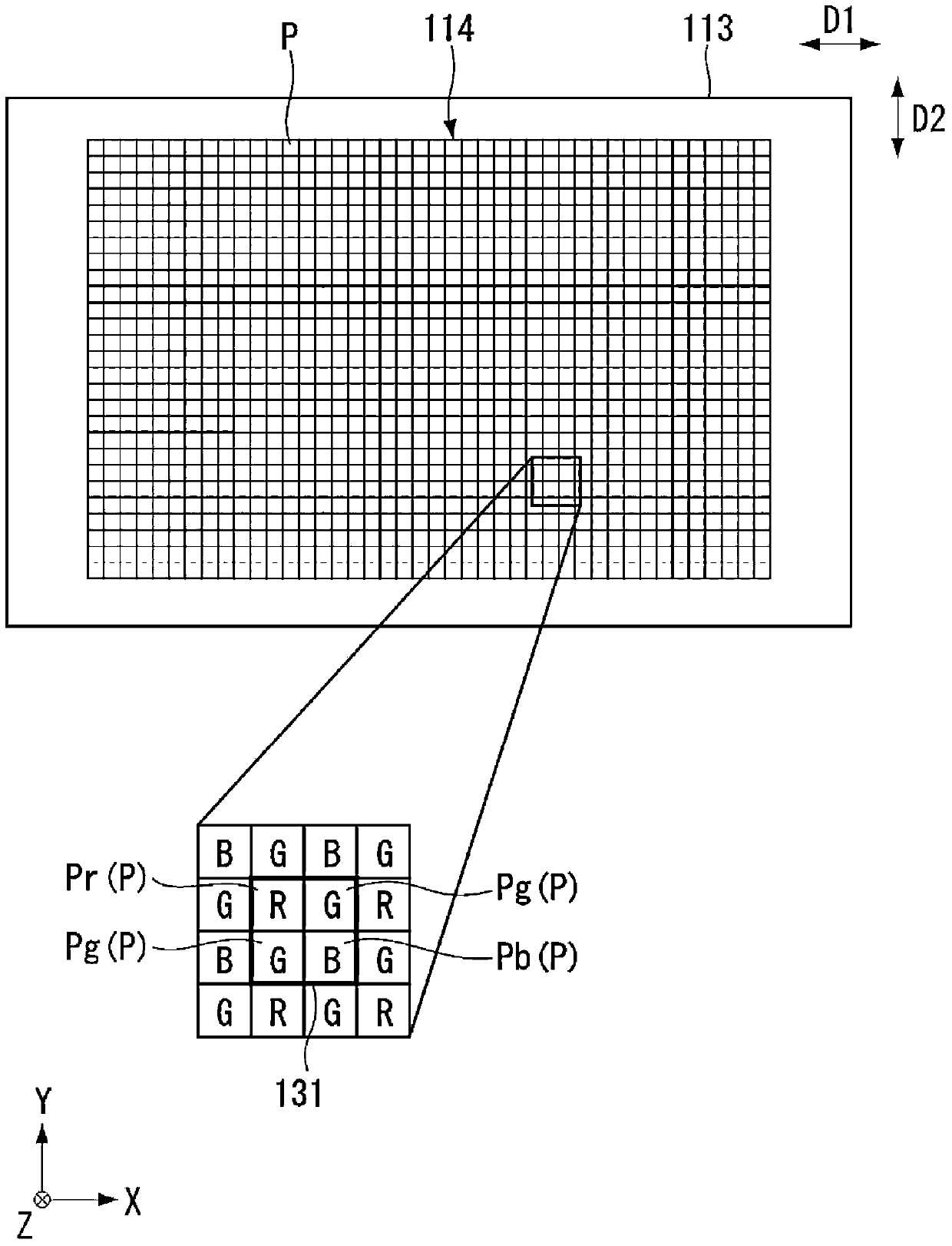
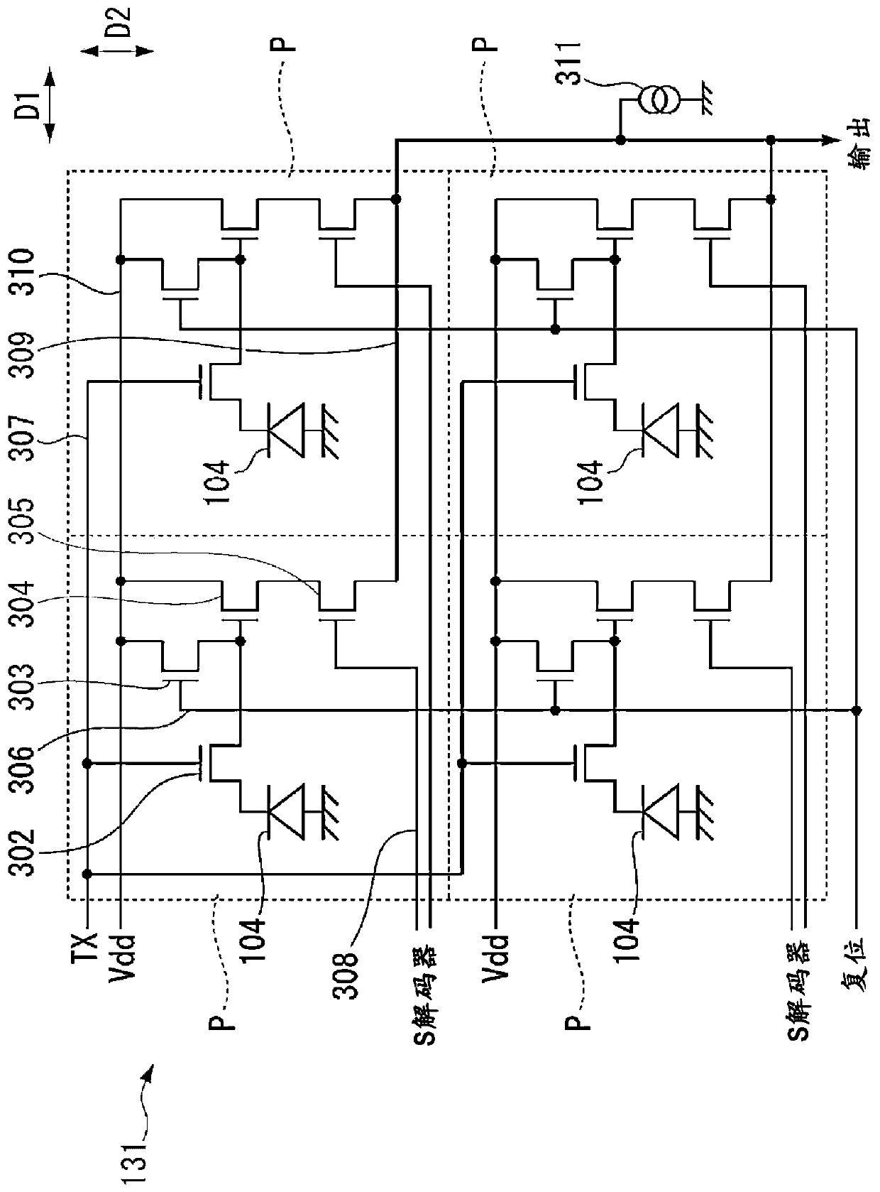
[0072] figure 1 It is a sectional view showing an example of the imaging element 100 . Such as figure 1 As shown, the imaging element 100 has an imaging chip 113 that outputs a pixel signal corresponding to incident light, a signal processing chip 111 that processes the pixel signal output from the imaging chip 113, and a memory chip 112 that stores the pixel signal processed by the signal processing chip 111. . The imaging chip 113, the signal processing chip 111, and the memory chip 112 are stacked. The imaging...
no. 2 approach -
[0179]
[0180] First, the multilayer imaging device 100 mounted on an electronic device (for example, imaging device 1 ) according to a second embodiment of the present invention will be described. In addition, this multilayer imaging device 100 is an invention described in Japanese Patent Application No. 2012-139026 previously proposed by the applicant of the present application. Figure 13 is a cross-sectional view of the multilayer imaging device 100 . The imaging element 100 has: a back-illuminated imaging chip 113 that outputs pixel signals corresponding to incident light; a signal processing chip 111 that processes pixel signals; and a memory chip 112 that stores pixel signals. These back-illuminated imaging chip 113 , signal processing chip 111 , and memory chip 112 are stacked and electrically connected to each other via conductive bumps 109 such as Cu (copper).
[0181] In addition, as shown in the figure, the incident light is mainly incident toward the positive ...
Deformed example 1
[0250] The imaging device 1 of the above-described embodiment can be constituted by a multifunctional mobile phone or a tablet terminal. In this case, an imaging unit mounted on a multifunctional mobile phone (or a tablet terminal) is configured using the above-described multilayer imaging element 100 .
PUM
 Abstract
Description
Claims
Application Information
 - R&D
- Intellectual Property
- Life Sciences
- Materials
- Tech Scout
- Unparalleled Data Quality
- Higher Quality Content
- 60% Fewer Hallucinations
Browse by: Latest US Patents, China's latest patents, Technical Efficacy Thesaurus, Application Domain, Technology Topic, Popular Technical Reports.
© 2025 PatSnap. All rights reserved.Legal|Privacy policy|Modern Slavery Act Transparency Statement|Sitemap|About US| Contact US: help@patsnap.com