
Semiconductor memory operation method

An operation method and memory technology, applied in static memory, read-only memory, digital memory information, etc., can solve the problems of increasing the total number of operation cycles, affecting system performance, consumption, etc., and achieving the effect of improving chip performance and reducing operation time.

Active Publication Date: 2016-06-15
INST OF MICROELECTRONICS CHINESE ACAD OF SCI
View PDF5 Cites 3 Cited by
  • Summary
  • Abstract
  • Description
  • Claims
  • Application Information

AI Technical Summary

Problems solved by technology

The operation of discontinuously reading data is similar, waiting for the random sequence unit to generate random codes will consume multiple cycles, increase the total number of operating cycles, and affect system performance

Method used

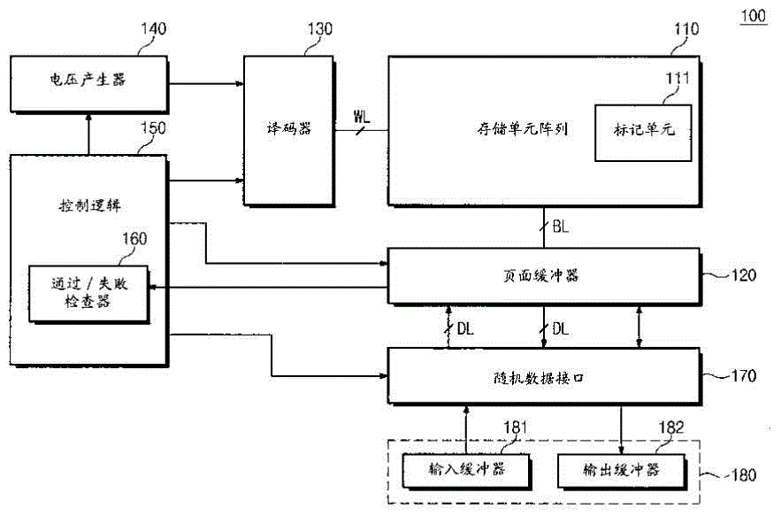
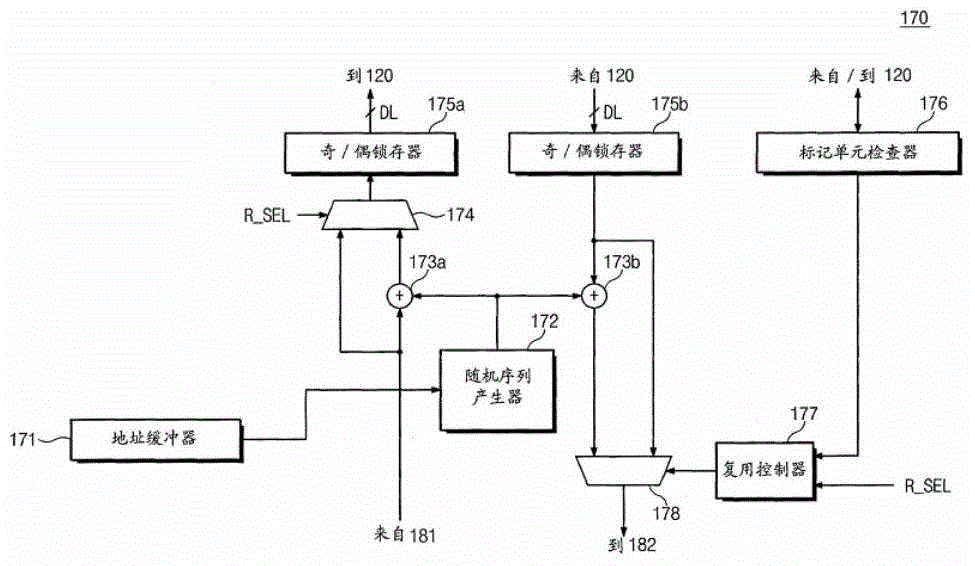
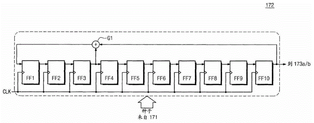

Image

  • Semiconductor memory operation method
  • Semiconductor memory operation method
  • Semiconductor memory operation method

Examples


Embodiment Construction

[0026] The features and technical effects of the technical solution of the present invention will be described in detail below with reference to the accompanying drawings and in conjunction with schematic embodiments, and a semiconductor memory operation method using combinational logic to form a random sequence generation unit to reduce operating time and improve chip performance is disclosed. It should be pointed out that similar reference numerals represent similar structures, and the terms "first", "second", "upper", "lower" and the like used in this application can be used to modify various device structures or manufacturing processes . These modifications do not imply spatial, sequential or hierarchical relationships of the modified device structures or fabrication processes unless specifically stated.

[0027] like figure 2 Shown is a structural diagram of the fast random code generating unit according to the present invention. The basic structure of the memory of th...


PUM


Abstract

A semiconductor memory operation method includes the following steps: randomizing operation address data to obtain a random code; performing combination logical operation to the random code to original data to obtain randomized data or performing combination logical operation to the randomized data with the random code to obtain de-randomized data; and storing the randomized data or outputting the de-randomized data. By means of the method, a random sequence generation unit is formed though combinatorial logic or non-iterative sequential logic, so that the method is free of awaiting a special period during an encoding / decoding process, reduces operation time and improves chip performance.

Description

technical field [0001] The invention relates to a method for operating a nonvolatile memory, in particular to a method for operating a NAND flash memory. Background technique [0002] Nonvolatile memory devices include flash memory, impedance variable memory devices, and the like. Flash memory may be classified into NAND flash memory and NOR flash memory. The structural feature of NOR flash memory is that its memory cells are connected in parallel to the bit lines. This parallel connection allows random access to the storage cells of the NOR flash memory. In contrast, the structure of NAND flash memory is characterized by its memory cells being serially connected to bit lines. That is, memory cells in NAND flash memory are connected into a string of memory cells, so only one connection tab to a bit line is required. Therefore, NAND flash memory can be very densely integrated. [0003] For a string of cells in the NAND flash memory, the programmed background pattern will...

Claims


Application Information

Patent Timeline
Patent Type & Authority Applications(China)
IPC IPC(8): G11C16/08
CPCG11C16/08G11C7/1012G11C16/10G11C16/26G11C16/0483G11C16/3427
Inventor 叶甜春
Owner INST OF MICROELECTRONICS CHINESE ACAD OF SCI
Learn More