MOS power device and method for forming same

A power device and device technology, applied in the field of MOS type power device and its formation, can solve the problems of optimization limitation, MOS type power device withstand voltage drop, etc., so as to reduce the on-voltage drop, improve the blocking effect, and alleviate the on-voltage The effect of drop and withstand voltage

Active Publication Date: 2016-06-01
BYD SEMICON CO LTD
View PDF4 Cites 0 Cited by
  • Summary
  • Abstract
  • Description
  • Claims
  • Application Information

AI Technical Summary

Problems solved by technology

According to semiconductor theory, the higher the doping concentration, the larger the electric field gradient, and the greater the slope of the electric field distribution in the hole blocking layer. As the depletion layer extends to the N-region, the electric field drops rapidly, resulting in the withstand voltage of MOS power devices. Significantly lower, the conduction voltage drop and the withstand voltage are mutually restricted, and the optimization is limited

Method used


Image

  • MOS power device and method for forming same
  • MOS power device and method for forming same
  • MOS power device and method for forming same

Examples


Embodiment Construction

[0026] Embodiments of the present invention are described in detail below, examples of which are shown in the drawings, wherein the same or similar reference numerals designate the same or similar elements or elements having the same or similar functions throughout. The embodiments described below by referring to the figures are exemplary and are intended to explain the present invention and should not be construed as limiting the present invention.

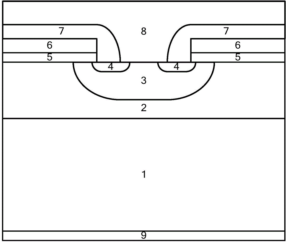
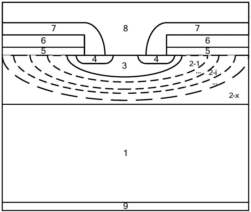
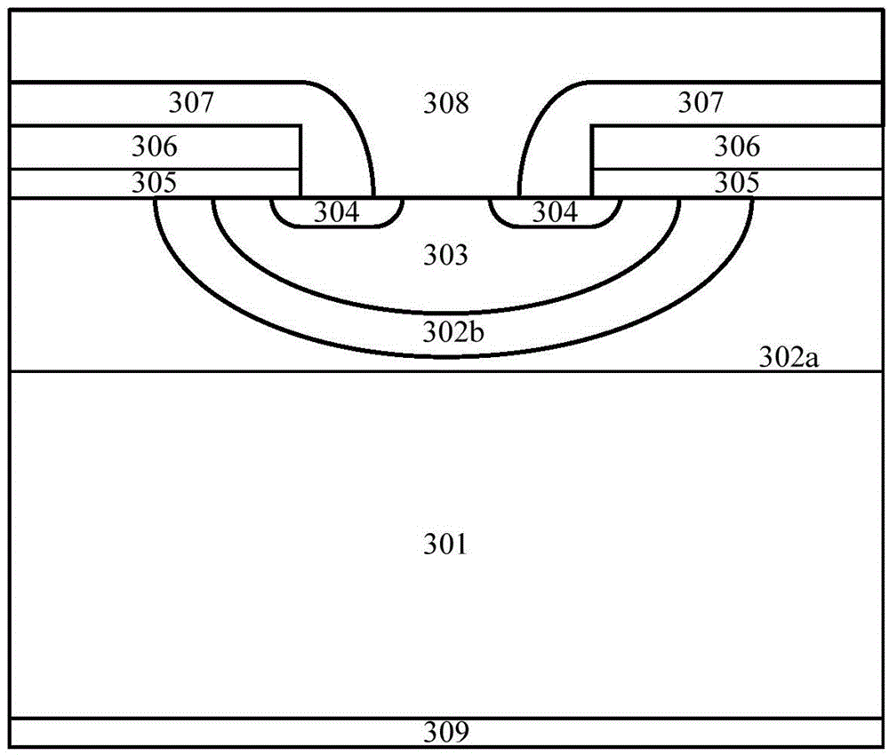
[0027] The MOS type power device of the embodiment of the present invention is such as figure 2 As shown, the following parts may be included: a voltage-resistant layer 1 of the first conductivity type; a barrier layer of the first conductivity type located on the voltage-resistant layer 1; a well region 3 of the second conductivity type located in the barrier layer; A source region 4 of the first conductivity type in the region 3; a first insulating layer 5 located on the barrier layer; a gate 6 located on the first insulating ...


PUM


Abstract

The invention discloses a MOS power device and a method for forming the same. The MOS power device comprises a first conductive type of voltage-withstand layer, a first conductive type of barrier layer on the voltage-withstand layer, a second conductive type of well region in the barrier layer, first conductive type of source regions in the well region, gates on the barrier layer, a first electrode on the gates and the barrier layer, and a second electrode under the voltage-withstand layer, wherein the barrier layer comprises multiple barrier child layers, the first barrier child layer wraps the well region, the (i+1)th barrier child layer wraps the ith barrier child layer, and the dosage concentration of the ith barrier child layer is greater than that of the (i+1)th barrier child layer. In the MOS power device, the barrier layer is a multi-child-layer structure with gradually changed dosage concentration. Equivalently, multiple barriers are provided so that the on-state voltage drop is decreased, low total amount of doped impurities is achieved, the withstand voltage of the MOS power device cannot be reduced obviously, and a restriction between the on-state voltage drop and the voltage-withstand capability is relieved.

Description

technical field [0001] The invention relates to the technical field of semiconductor manufacturing, in particular to a MOS type power device and a forming method thereof. Background technique [0002] MOS type power devices with conductance modulation effect are widely used in medium, high voltage, medium and high frequency fields due to their advantages such as reduced conduction voltage and fast switching speed. Low loss has always been an important goal for the development of semiconductor MOS power devices, and lower conduction voltage drop ensures that MOS power devices have lower conduction losses. For MOS power devices with conductance modulation effect, the near-surface carrier storage technology is an effective means to reduce the on-voltage drop, and the hole blocking layer structure is the most common type of surface carrier storage technology. The specific solution is: introduce a layer of N-type doping region with higher doping concentration than N- in the part...

Claims


Application Information

Patent Timeline
Patent Type & Authority Applications(China)
IPC IPC(8): H01L29/78H01L21/336
Inventor 吴海平肖秀光刘鹏飞
Owner BYD SEMICON CO LTD
Why Eureka
Try Eureka