tft and manufacturing method, array substrate, display panel and driving method, display device

A display panel and substrate substrate technology, which is applied in static indicators, cathode ray tube indicators, semiconductor/solid-state device manufacturing, etc., can solve the problems of high power consumption of display devices, save working power, reduce power consumption, etc. consumption effect

Inactive Publication Date: 2019-05-03
BOE TECH GRP CO LTD +1
View PDF6 Cites 0 Cited by
  • Summary
  • Abstract
  • Description
  • Claims
  • Application Information

AI Technical Summary

Problems solved by technology

[0003] However, since the ambient light sensor must be installed in the display device, and it needs to provide working power for the ambient light sensor, the overall power consumption of the display device is relatively large.

Method used


Image

  • tft and manufacturing method, array substrate, display panel and driving method, display device
  • tft and manufacturing method, array substrate, display panel and driving method, display device
  • tft and manufacturing method, array substrate, display panel and driving method, display device

Examples


Embodiment Construction

[0043] In order to further illustrate the TFT and its manufacturing method, array substrate, display panel, driving method, and display device provided by the embodiments of the present invention, the following description will be made in detail with reference to the accompanying drawings.

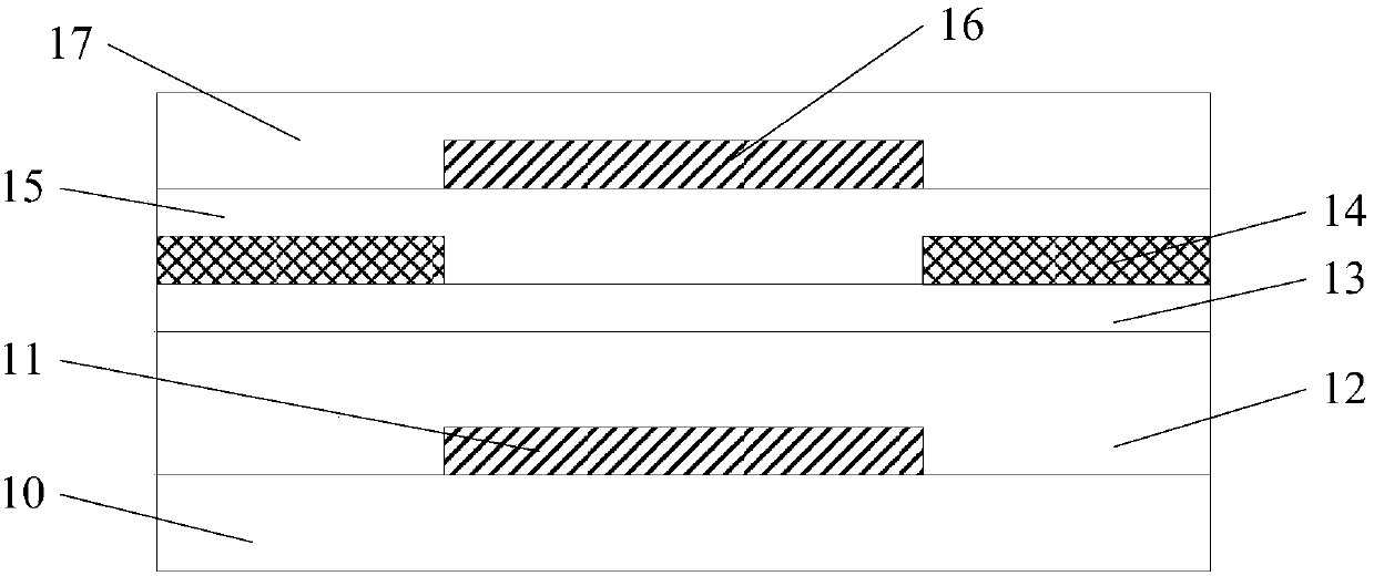
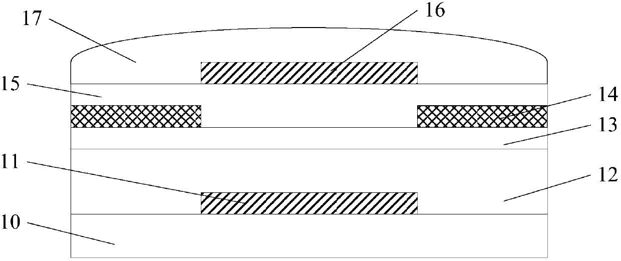
[0044] see figure 1 The TFT (Thin Film Transistor, TFT) provided by the embodiment of the present invention includes a base substrate 10, on which a first gate 11, a bottom gate dielectric layer 12 and an insulating layer 13 are sequentially stacked, and the A source electrode and a drain electrode 14 are provided on the insulating layer 13, and a top gate dielectric layer 15, a second gate electrode 16 and a passivation layer 17 are sequentially stacked on the source electrode, the drain electrode 14 and the insulating layer 13; that is In other words, the TFT in the embodiment of the present invention has a double-gate structure, wherein the first gate 11 or the second gate 16 is a photo...


PUM


Abstract

The invention discloses a TFT, a manufacturing method, an array substrate, a display panel, a driving method, and a display device, and relates to the field of display technology, in order to solve the problem of large overall power consumption of the display device. The TFT includes a base substrate, on which a first gate, a bottom gate dielectric layer and an insulating layer are sequentially stacked, a source and a drain are arranged on the insulating layer, and a source and a drain are arranged on the base substrate. A top gate dielectric layer, a second gate and a passivation layer are sequentially stacked on the insulating layer; the first gate or the second gate is a photosensitive material gate. The TFT and the display panel provided by the invention are applied to a display device.

Description

technical field [0001] The invention relates to the field of display technology, in particular to a TFT and a manufacturing method, an array substrate, a display panel, a driving method, and a display device. Background technique [0002] At present, display devices are more and more used in people's work, study and entertainment. When users use display devices in different scenarios, the intensity of ambient light around the display devices in different scenarios is often different. In order to be able to adjust For the brightness of the display screen of the display device, an ambient light sensor is often installed in the display device, and the brightness information of the ambient light is obtained through the ambient light sensor, and the brightness information is provided to the processing module of the display device, and the processing module performs the processing according to the acquired brightness information. The brightness information of the ambient light is ...

Claims


Application Information

Patent Timeline
Patent Type & Authority Patents(China)
IPC IPC(8): G02F1/1368G02F1/133G09G3/36
CPCG02F1/13306G02F1/1368G09G3/3648G02F1/136295H01L31/095H01L31/173H01L31/109G09G2320/0626G09G2330/021G09G2330/12G09G2360/144H01L29/78648H01L29/4908H01L29/78663H01L29/6675H01L27/1248G09G3/36G09G5/10G09G2320/08H01L21/02532H01L21/02592H01L27/1222H01L27/124H01L27/1262H01L31/09H01L31/161
Inventor 张斌董殿正张衎陈鹏名
Owner BOE TECH GRP CO LTD
Why Eureka
Try Eureka