Storage element, developing cartridge employing same and image forming equipment

A technology for storage elements and developing cartridges, which is applied in the fields of electric recording process equipment using charge patterns, electric recording technology using charge patterns, and electric recording techniques, etc., which can solve the problem of affecting the stability of storage elements and affecting the components on the storage elements. Lifespan, damaged components and other issues

Inactive Publication Date: 2016-05-04
ZHUHAI PANTUM ELECTRONICS
View PDF9 Cites 13 Cited by
  • Summary
  • Abstract
  • Description
  • Claims
  • Application Information

AI Technical Summary

Problems solved by technology

However, during the process of installing the developing cartridge into the printer, if the signal contacts (SDA, SCL) on the storage element are in contact with the corresponding contacts of the printer body before the voltage contacts (VCC), it is possible that the voltage contacts ( VCC) and the signal contacts (SDA, SCL) form a reverse large current, that is, the current flows from the SDA contact and the SCL contact to the VCC contact through multiple components inside the storage element, thereby affecting the components on the storage element life, or even damage components, affecting the stability of storage components
When the developer cartridge is taken out of the printer, if the voltage contact (VCC) on the storage element is disconnected from the corresponding contact of the printer body before the signal contact (SDA, SCL), the above problems will also occur and affect the storage element. job stability

Method used


Image

  • Storage element, developing cartridge employing same and image forming equipment
  • Storage element, developing cartridge employing same and image forming equipment
  • Storage element, developing cartridge employing same and image forming equipment

Examples


Embodiment 1

[0060] figure 2 Shown is a schematic diagram of the overall structure of an imaging device provided in this embodiment. The image forming apparatus 100 includes an image forming apparatus main body 101 , a developing cartridge 102 , a paper feed roller 103 and a fixing assembly 104 . Among them, the developing cartridge 102 is used to form an image and transfer the image to a recording medium. The developing cartridge 102 is detachably installed in the imaging device, and a storage element is installed on the developing cartridge for recording the developing cartridge information and imaging control parameters. The main body of the imaging device 101 communicates with the developing cartridge by electrically connecting with the storage element on the developing cartridge 102 , for example, reading the information and control parameters of the developing cartridge in the storage element, or writing the usage information of the developing cartridge into the storage element. T...

Embodiment 2

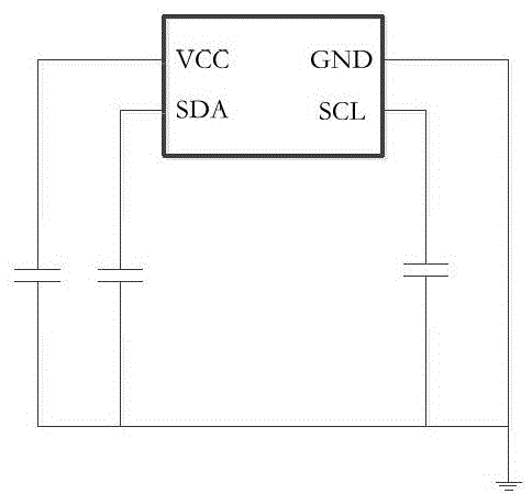
[0076] Such as Figure 7 As shown, the storage element 600 in this embodiment includes a storage element substrate 610, and a positioning notch 620 for positioning and a plurality of contacts are provided on the storage element substrate 610 . Different from Embodiment 1, the plurality of contacts on the storage element substrate in this embodiment are arranged in a row parallel to the axis of the photosensitive drum, and the plurality of contacts in this embodiment include GND contact 611, VCC contact Point 612 , signal contact 613 and signal contact 614 . The number of signal contacts provided by this embodiment is not limited to Figure 7 Two of them can also be set to 1 or more than 2.

[0077] Such as Figure 8 Shown is a schematic diagram of the contact arrangement method of the storage element in this embodiment. The height of the contact portion of the GND contact 711 is higher than that of other contacts, and the height of the contact portion of the VCC contact 71...

Embodiment 3

[0083] Figure 9 It is a partial schematic diagram of the main body of the imaging device in this embodiment. As shown in the figure, a straight line L3 in the figure indicates the axis of the photosensitive drum as a rotating member in the developing cartridge when the developing cartridge is installed in the image forming apparatus. The rotating element is not limited to the photosensitive drum, and in other embodiments may also be elements such as developing rollers or protrusions provided at both ends of the developing cartridge. The X2, Y2, and Z2 directions in the figure represent three axial directions in which the main body of the imaging device is located in a Cartesian coordinate system, respectively.

[0084] The main body 800 of the image forming apparatus is provided with a plurality of contact pieces contacting with the storage element of the developing cartridge, and the plurality of contact pieces are arranged in two rows. The contact element may be a conduct...


PUM


Abstract

The invention discloses a storage element for a developing cartridge, the developing cartridge comprising the storage element and image forming equipment comprising the developing cartridge. When the developing cartridge is arranged on the image forming equipment, conduction of a grounding contact on the storage element and a corresponding contact element in a main body of the image forming equipment is before conduction of a voltage contact on the storage element and the corresponding contact element in the main body; and conduction of the voltage contact on the storage element and the corresponding contact element in the main body is before conduction of a signal contact on the storage element and the corresponding contact element in the main body. The storage element disclosed by the invention can avoid the problem that components on the storage element are damaged due to the fact that high voltages are formed on the contacts on the storage element to discharge; and furthermore, the problem that the storage element of the developing cartridge is poor in stability when working due to the fact that a plurality of contacts on the storage element and a plurality of corresponding contacts on the main body of the image forming equipment do not have a certain successive contact order can be solved.

Description

technical field [0001] The invention relates to the technical field of imaging, in particular to a storage element, a developing cartridge using the storage element, and an image forming device. Background technique [0002] A printer or an image forming device with a printing function (hereinafter referred to as an imaging device) is a common office device and is gradually becoming a household electronic device. Most existing laser printers use detachable developing cartridges (or toner cartridges, toner cartridges, etc.) to form images on recording media. During normal use, the developing cartridges are installed in the printer. The developing cartridges contain storage elements, and the storage elements are provided with storage units. , the storage unit can store information such as model, capacity, use area, etc. of the developing cartridge. The main body of the printer is provided with a contact piece that is in contact with the storage element of the developer cartri...

Claims


Application Information

Patent Timeline
IPC IPC(8): G03G15/08G03G21/18
CPCG03G15/08G03G21/1885
Inventor 尹爱国黄超豪万立
Owner ZHUHAI PANTUM ELECTRONICS
Why Eureka
Try Eureka