
Array base plate, preparation method thereof and display panel

A technology of array substrate and base substrate, which is applied in the fields of display panel, its preparation and array substrate, and can solve problems such as defectiveness

Inactive Publication Date: 2016-04-20
BOE TECH GRP CO LTD +1
View PDF8 Cites 14 Cited by
  • Summary
  • Abstract
  • Description
  • Claims
  • Application Information

AI Technical Summary

Problems solved by technology

[0004] In view of this, an embodiment of the present invention provides an array substrate, its preparation method and a display panel, which are used to improve the bad problems caused by the via depth of the insulating layer in the existing array substrate.

Method used


Image

  • Array base plate, preparation method thereof and display panel
  • Array base plate, preparation method thereof and display panel
  • Array base plate, preparation method thereof and display panel

Examples


preparation example Construction

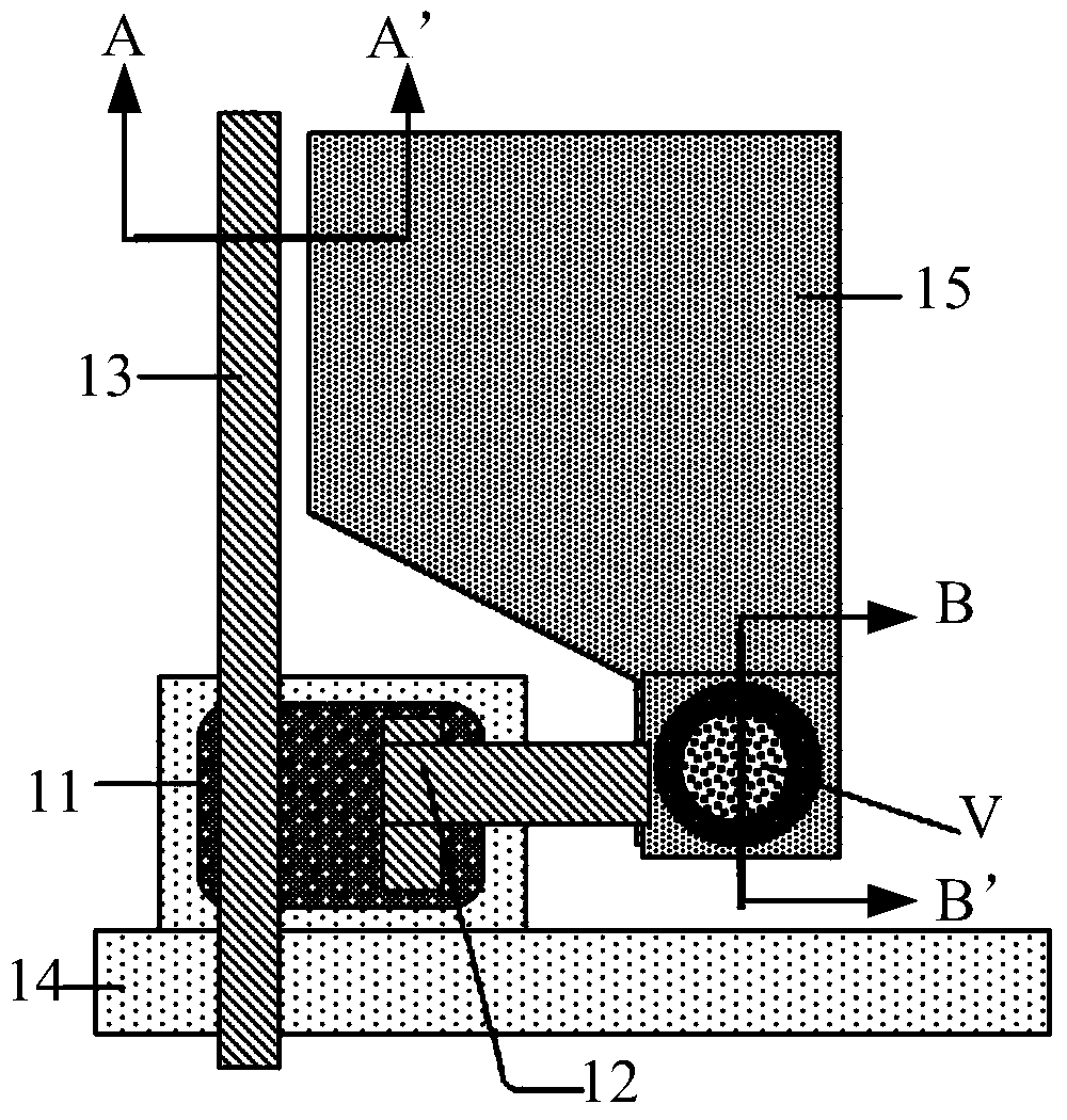
[0062] Based on the same inventive concept, an embodiment of the present invention also provides a method for preparing any one of the above-mentioned array substrates, such as Image 6 As shown, the following steps may be included:

[0063] S601, forming a pattern of the first conductive layer on the base substrate;

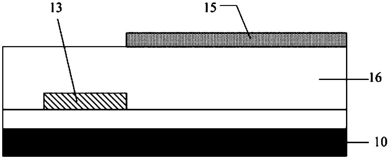
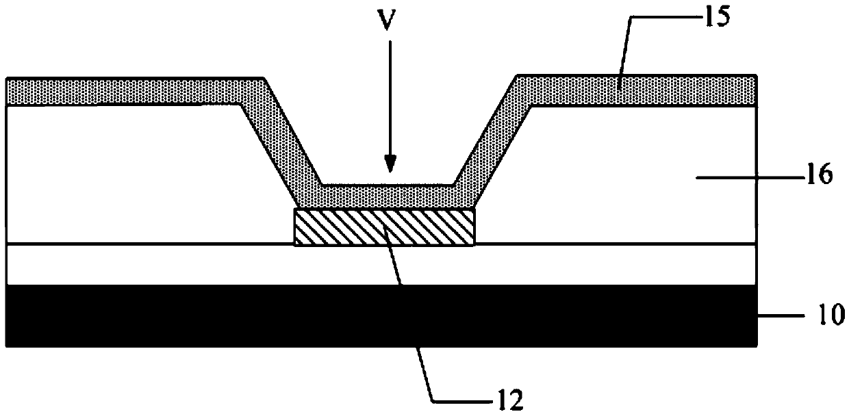
[0064] S602, forming a pattern of an insulating layer on the base substrate formed with the first conductive layer; wherein, the insulating layer has a via area, a semi-reserved area outside the via area, and a pattern surrounding the semi-reserved area and the via area The fully reserved area of ​​the area, the via area is a via hole penetrating the insulating layer, and the vertical distance between the upper surface of the semi-reserved area of ​​the insulating layer and the upper surface of the first conductive layer is smaller than the upper surface of the fully reserved area of ​​the insulating layer the vertical distance from the upper surface of the fir...


PUM

PropertyMeasurementUnit
Widthaaaaaaaaaa
Thicknessaaaaaaaaaa

Abstract

The invention discloses an array base plate, a preparation method thereof and a display panel. The array base plate comprises a substrate base plate and a first conducting layer, an insulating layer and a second insulating layer which are sequentially located on the substrate base plate, the insulating layer is provided with a via hole area, a semi-preservation area located on the outer side of the via hole area and a total-preservation area surrounding the area where the semi-preservation area and the via hole area are located. Due to the fact that the surrounding area of the via hole area is the semi-preservation area, the thickness of the insulating layer surrounding a via hole is lowered, it can be guaranteed that the size of the via hole is reduced under the situation that the via hole gradient is fixed, accordingly the opening rate is raised, and the influence of residual insulating layer materials on the edge of the via hole can be lowered; besides, the height range difference of the insulating layer is divided into two segments, so that the range difference influence caused by the overall thickness of the insulating layer can be lowered.

Description

technical field [0001] The invention relates to the field of display technology, in particular to an array substrate, its preparation method and a display panel. Background technique [0002] In the thin film transistor liquid crystal display (ThinFilmTransistorLiquidCrystalDisplay, TFT-LCD) production process, since the organic insulating film layer is easy to form a thicker film layer, it can reduce signal interference in the array substrate, reduce parasitic capacitance, reduce substrate load and thus reduce Power consumption and other advantages, so the organic insulating film layer is widely used. Usually, the organic insulating film layer is disposed between two conductive film layers, for example, between the source-drain electrode layer and the pixel electrode layer. In order to electrically connect the pixel electrode to the drain of the thin film transistor, a via hole (ViaHole) needs to be formed on the organic insulating film layer. [0003] Such as Figure 1a ...

Claims


Application Information

Patent Timeline
IPC IPC(8): H01L27/12H01L21/77H01L21/768G02F1/1362
CPCG02F1/1362H01L21/768H01L21/76802H01L21/77H01L27/12H01L27/1214H01L27/02G02F1/136227H01L27/1244G02F1/134309G02F1/136259G02F1/136286H01L21/28008H01L27/1248H01L29/78633
Inventor 陈程李纪龙徐德智吕艳明
Owner BOE TECH GRP CO LTD
Learn More