Integrated circuit package structure and manufacturing technology thereof

A technology of integrated circuit and packaging structure, which is applied in the direction of circuits, electrical components, and electrical solid devices, and can solve the problems of large thickness of QFN/DFN products, and achieve the effects of shortening the design cycle, increasing the bonding area, and dense I/O

Inactive Publication Date: 2016-04-20
GUANGDONG CHIPPACKING TECH
View PDF3 Cites 3 Cited by
  • Summary
  • Abstract
  • Description
  • Claims
  • Application Information

AI Technical Summary

Problems solved by technology

[0003] In order to overcome the shortcomings of the traditional QFN process that the thickness of QFN / DFN products is still relatively large and cannot meet the needs of current portable devices for small volume and high-density packaging, the present invention provides a film-free and electroplating-free technology based on bonding wire connection. Integrated circuit packaging structure and its production process

Method used


Image

  • Integrated circuit package structure and manufacturing technology thereof
  • Integrated circuit package structure and manufacturing technology thereof
  • Integrated circuit package structure and manufacturing technology thereof

Examples


Embodiment Construction

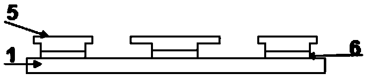
[0031] Such as Figure 9 As shown, a film-free and electroplating-free package based on bonding wire connection also includes metal bumps 2 . The chamfered silver-plated layer 5 is a mutually independent silver-plated layer segment, a part of the chamfered silver-plated layer 5 has a chip 3, and a part of the chamfered silver-plated layer 5 has a metal bump 2, and the chip 3 and the metal bump The point 2 is connected by the bonding wire 7, the plastic package 4 surrounds the metal bump 2, the chip 3, the chamfered silver-plated layer 5, the nickel-palladium-gold layer 6 and the bonding wire 7, the metal bump 2, the chip 3, the chamfered Angle silver plated layer 5, nickel palladium gold plated layer 6 and bonding wire 7 constitute the power supply and signal channel of the circuit. Such as Figure 13 As shown, a film-free and electroplating-free package based on bonding wire connection can also be used without metal bumps, and the bonding wire can be directly hit on the pad...


PUM


Abstract

The invention provides an integrated circuit package structure and a manufacturing technology thereof, and the structure is film-pasting-free and electroplating-free and is based on the bonding wire connection. The structure comprises a silver plating layer which is mutually independent silver plating layer sections and chips which are arranged on some silver plating layer sections, the silver plating layer sections are connected through bonding wires, plastic package bodies are arranged on the peripheries of the chips, the silver plating layer, a nickel-palladium-gold plating layer and the bonding wires, and a power supply and a signal channel are formed by the chips, the silver plating layer, the nickel-palladium-gold plating layer and the bonding wires. The invention also provides the manufacturing technology of the above integrated circuit packaging, the packaging part provided by the invention is film-pasting-free and electroplating-free, so that the production cost can be greatly reduced, the product is more competitive than the prior art. The manufacturing technology is suitable for applying in integrated circuit packaging.

Description

technical field [0001] The invention belongs to the technical field of integrated circuit packaging, and more specifically relates to a film-free and electroplating-free production process based on bonding wire connection. Background technique [0002] Integrated circuit flat no-lead packaging (QFN / DFN), in recent years, with communication equipment (such as base stations, switches), smart phones, portable devices (such as tablet computers), wearable devices (such as smart watches, smart glasses, Smart bracelets, etc.) are popularized and developed rapidly, and are especially suitable for the packaging of large-scale integrated circuits with electrical requirements such as high frequency, high bandwidth, low noise, high thermal conductivity, small volume, and high speed. Integrated circuit flat no-lead packaging (QFN / DFN) effectively utilizes the packaging space of the lead pins, thereby greatly improving the packaging efficiency. Due to the short leads, small size of the p...

Claims


Application Information

Patent Timeline
Patent Type & Authority Applications(China)
IPC IPC(8): H01L23/495H01L23/488H01L21/60
CPCH01L21/568H01L23/3121H01L23/4952H01L23/49548H01L23/49582H01L2224/48H01L2224/48091H01L2224/48247H01L2224/48249H01L2224/83439H01L2224/85H01L2224/85001H01L2224/85439H01L2924/181H01L2924/18301H01L2924/00014H01L2924/00012H01L2924/00H01L23/495H01L23/488H01L24/85
Inventor 刘兴波梁大钟宋波
Owner GUANGDONG CHIPPACKING TECH
Why Eureka
Try Eureka