Microphone printed circuit board (pcb) high in utilization rate and lower punching die structure thereof

A technology of pcb board and utilization rate, which is applied in the field of micro-head pcb board and its stamping die structure, can solve the problems of low utilization rate of base material and increase of raw material cost, and achieve low stamping cost, high utilization rate and significant economic benefits Effect

Inactive Publication Date: 2016-04-13
苏州市三生电子有限公司
View PDF5 Cites 2 Cited by
  • Summary
  • Abstract
  • Description
  • Claims
  • Application Information

AI Technical Summary

Problems solved by technology

[0002] In the circuit board, the switches of the produced microphone products are all reflected on the base material, and the number of panels for the CAM data operation is 320 small microphones, and the punching die is designed with 4 punch positioning holes to complete the positioning; its layout The utilization rate of the base material of the circuit board with through holes is low, which increases the cost of raw materials, and this type of circuit board needs secondary stamping, and the process positioning round hole and the process positioning waist hole for positioning on the edge of the forming board need to be stamped once , the second stamping is used to form pcb microphone products

Method used


Image

  • Microphone printed circuit board (pcb) high in utilization rate and lower punching die structure thereof
  • Microphone printed circuit board (pcb) high in utilization rate and lower punching die structure thereof
  • Microphone printed circuit board (pcb) high in utilization rate and lower punching die structure thereof

Examples


Embodiment Construction

[0018] The present invention will be described in detail below with reference to the accompanying drawings and in combination with embodiments.

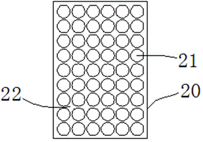
[0019] refer to figure 1 and figure 2 As shown, a microphone pcb board with high utilization rate and its stamping lower die 10 structure, it comprises a microphone pcb substrate 20 and a stamping lower die 10, and the microphone pcb substrate 20 is provided with a microphone unit 21 and a side Corner surplus material 22, described stamping lower die 10 is provided with upper left reference limit angle block 11, right upper reference limit angle block 12 and lower limit block 13, described left upper reference limit angle block 11, right upper reference limit angle block The block 12 and the lower limit block 13 wrap and position the peripheral edge of the microphone pcb substrate 20 .

[0020] like figure 2 As shown, the microphone units 21 are neatly and evenly arranged in a dot matrix, and the distance between the outermost m...


PUM


Abstract

The invention discloses a microphone printed circuit board (pcb) high in utilization rate and a lower punching die structure thereof. The microphone pcb comprises a microphone pcb base material and a lower punching die. The microphone pcb base material is provided with a microphone unit and leftovers. The lower punching die is provided with an upper left basic limiting angle block, an upper right basic limiting angle block and a lower limiting check block. The upper left basic limiting angle block, the upper right basic limiting angle block and the lower limiting check block are used for wrapping and positioning the periphery of the microphone pcb base material. The microphone pcb is free of technological plate edges required by a conventional circuit board base material, the punching process for positioning basic holes is eliminated, and the finished microphone pcb is directly formed; the number of punching procedures is small, the punching cost is low, the utilization rate of pcb materials is increased, and economic benefits are remarkable.

Description

technical field [0001] The invention relates to the field of stamping and forming of circuit boards, in particular to a microphone PCB board with high utilization rate and its stamping lower die structure. Background technique [0002] In the circuit board, the switches of the produced microphone products are all reflected on the base material, and the number of the CAM data operation panel is 320 small microphones, and the punching die is designed with 4 punch positioning holes to complete the positioning; its layout The utilization rate of the base material of the circuit board with through holes is low, which increases the cost of raw materials, and this type of circuit board needs secondary stamping, and the process positioning round hole and the process positioning waist hole for positioning on the edge of the forming board need to be stamped once , the second stamping is used to form pcb microphone head products. Contents of the invention [0003] The purpose of the...

Claims


Application Information

Patent Timeline
Patent Type & Authority Applications(China)
IPC IPC(8): B21D37/10B21D43/00
Inventor 孙祥根
Owner 苏州市三生电子有限公司
Why Eureka
Try Eureka