Semiconductor testing circuit and method for detecting conductive properties of tested piece

A technology for testing circuits and detection methods, which is applied in the field of semiconductors, and can solve problems such as the increase in resistance value, Joule heat, and the inability to test the resistance value of resistance

Inactive Publication Date: 2016-03-30
SEMICON MFG INT (SHANGHAI) CORP
View PDF5 Cites 8 Cited by
  • Summary
  • Abstract
  • Description
  • Claims
  • Application Information

AI Technical Summary

Problems solved by technology

However, with the development of semiconductor technology, the size of integrated circuit devices has become smaller and smaller, which has resulted in narrower and narrower widths of metal and polysilicon, which has caused a sharp increase in the resistance value of resistors, while the existing testing machines There is a certain allowable range for power, current, and voltage. If it exceeds the above allowable range, the resistance value of the resistor cannot be tested.
For example, the power upper limit, voltage upper limit, and current upper limit of a test machine are 2W, 2V, and 1mA respectively. The power of the test machine may not be fully used for testing resistance. Tested on the above test machine
In addition, Joule heat will be generated during the above test process, which will further cause the resistance of the tested piece to drift in the direction of increasing

Method used


Image

  • Semiconductor testing circuit and method for detecting conductive properties of tested piece
  • Semiconductor testing circuit and method for detecting conductive properties of tested piece
  • Semiconductor testing circuit and method for detecting conductive properties of tested piece

Examples


Embodiment Construction

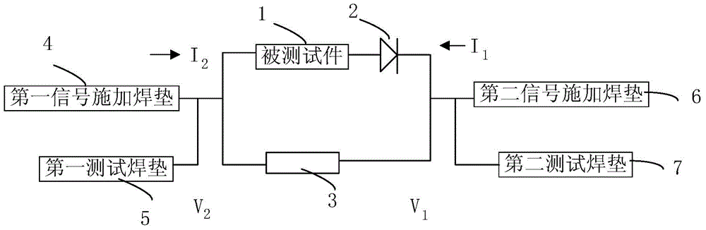
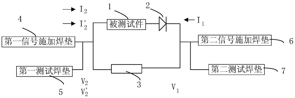
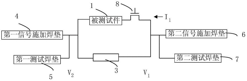
[0030] As mentioned in the background technology, for a test piece with a large resistance value, on the one hand, the test machine in the prior art has a certain allowable range due to power, current, and voltage. If it exceeds the above allowable range, the resistance value of the resistor cannot be tested. On the other hand, due to the large resistance and high heat generation, it affects the resistance value of the tested piece itself, making the test results inaccurate. In order to solve the above-mentioned technical problems, the present invention provides the following test circuit: the device under test is connected in series with the switch; a resistor is connected in parallel with the series circuit of the device under test and the switch; The pad is connected to one end of the parallel circuit; the second signal application pad and the second test pad are connected to the other end of the parallel circuit; the first signal application pad, the first test pad, the sec...


PUM


Abstract

The invention discloses a semiconductor testing circuit and a method for detecting conductive properties of a tested piece. The semiconductor testing circuit comprises the tested piece, a resistor, a first signal-applying welding pad, a first test welding pad, a second signal-applying welding pad and a second test welding pad, wherein the tested piece is connected with a switch in series; the resistor is parallelly connected with a series circuit of the tested piece and the switch; the first signal-applying welding pad and the first test welding pad are connected to one end of the parallel circuit; the second signal-applying welding pad and the second test welding pad are connected to the other end of the parallel circuit; and the first signal-applying welding pad, the first test welding pad, the second signal-applying welding pad and the second test welding pad form four ends of a Kelvin Contact. When in test, the switch is switched off firstly, the Kelvin Contact is adopted to obtain a resistance value of the additionally arranged resistor, then the switch is switched on, the Kelvin Contact is further adopted to obtain a total resistance value of the tested piece and the additionally arranged resistor after parallel connection, and the resistance value of the tested piece can be obtained accurately by separating the resistance value of the additionally arranged resistor from the total resistance value.

Description

technical field [0001] The invention relates to the technical field of semiconductors, in particular to a semiconductor test circuit and a method for detecting the conductivity of a tested piece. Background technique [0002] Electromigration (EM) will occur during the use of metal interconnect lines, and stress migration (StressMigration, SM) will occur during the use of metal or polysilicon. These two phenomena will affect the resistance value of the resistor. , resulting in device reliability problems. The phenomenon of electromigration means that when a high-density current passes through a metal material, the high-speed moving electron flow promotes the directional migration of the metal atoms, and the high-speed moving electrons collide with the metal atoms inelastically. During the collision, the electrons transfer part of the energy to the atoms, thereby As a result, the atoms move along the direction of electron movement, macroscopically, some areas appear voids, a...

Claims


Application Information

Patent Timeline
Patent Type & Authority Applications(China)
IPC IPC(8): G01R31/26
Inventor 徐孝景宋永梁吕勇
Owner SEMICON MFG INT (SHANGHAI) CORP
Why Eureka
Try Eureka